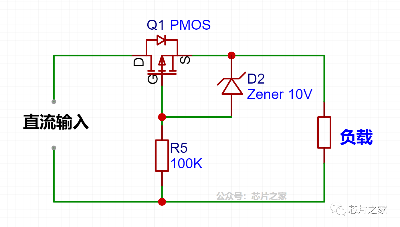
1. Anti reverse connection protection (diode)
In actual electronic design, anti reverse connection protection circuits are very important. Do not think that you will definitely not make mistakes. In fact, no matter how careful you are, you will still make mistakes
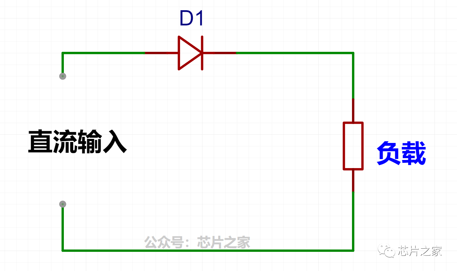

2. Anti reverse connection protection (PMOS)
The method of using diodes to prevent reverse connections was introduced above, but voltage drop is a pain point. Is there any way to remove this voltage drop? PMOS is here!
We know that after complete conduction of PMOS, the conduction resistance is very small, with a typical few hundred milliohms and some tens of milliohms. We have added a Zener diode between the GS to prevent the input voltage from exceeding the Vgs of the MOS. The Vgs rated value is 20V, and we usually use 10V to meet this requirement. The specific selection of Zener diodes is based on the actual characteristics of the MOS.
Principle analysis: When a forward voltage is applied to the input terminal, such as+5V, the voltage at the D terminal is 5V. Due to the presence of MOSFET diodes, the voltage at the S terminal is 4.3V. The voltage at the S terminal minus the voltage at the G terminal is greater than the on voltage. After the PMOS conducts, the parasitic diode shortcircuits and no longer works; After the voltage is reversed, the voltage at the G terminal is greater than the voltage at the S terminal and does not conduct, achieving the function of preventing reverse connection.
The circuit is simple, but there is a problem with this circuit, it will reverse. Assuming that the load on the right side is a battery with a voltage of Vb, when the DC input suddenly disconnects, Q1's Vgs meets the MOS conduction condition, PMOS will conduct, and the current will flow back from the right to the left, which may cause some unknown faults.
Although diodes do not have reverse current (strictly speaking, there is leakage current), there is reverse current. If the load has a large capacity capacitor or battery, when the input terminal is turned off, the current will flow out from the load terminal from right to left. Of course, there is no problem using this circuit in simple circuit situations.
3. DC surge current suppression switch
This circuit can solve the problem of large capacity capacitors in the load and huge surge current at the power supply end. Slowly increase the voltage during startup to suppress the surge current during power on.
The time for voltage increase is determined by C1 and R6 in the figure. As the value increases, the slow start time becomes longer. Of course, a Zener diode can also be added between GS according to the method in the second point.
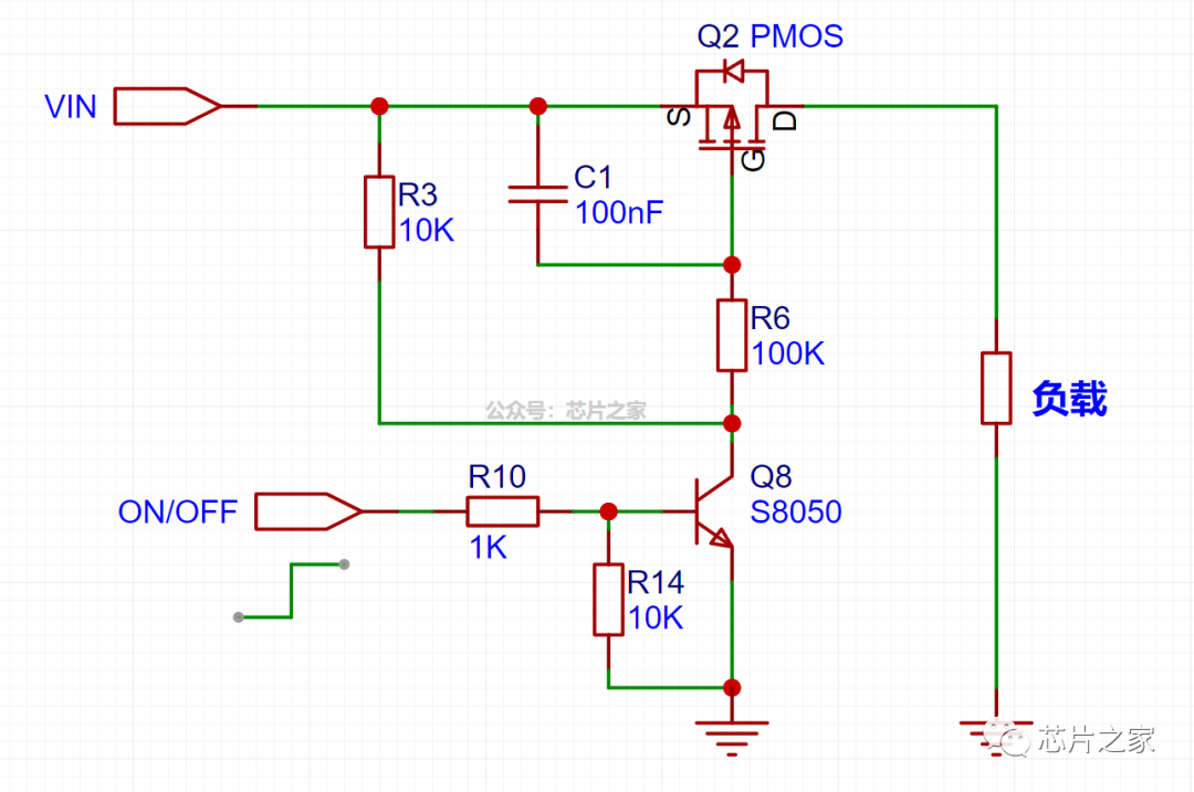
If no switch is needed, the transistor part can be removed and only the slow start function can be used.
4. Back-to-back anti backflow
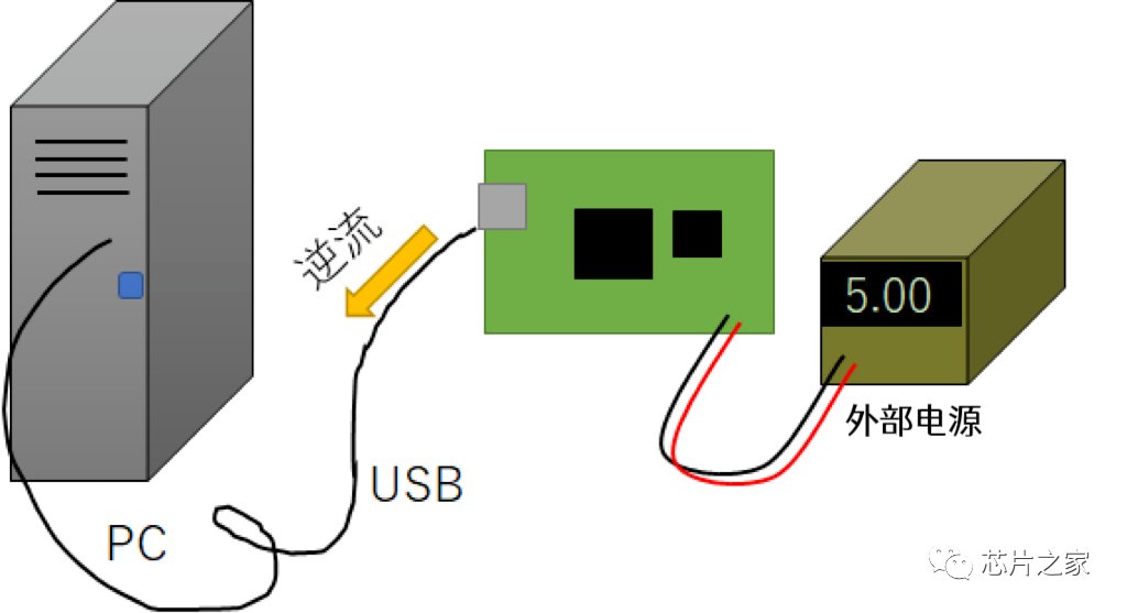
As mentioned in the anti reverse connection protection circuit in the second point, there is a risk of backflow, especially when the load end is a battery or has a large capacity capacitor, or when the computer's USB is used for debugging and there is an external power supply, it may flow to Vin testing, which may cause a series of faults. So, is there any way to prevent backflow?
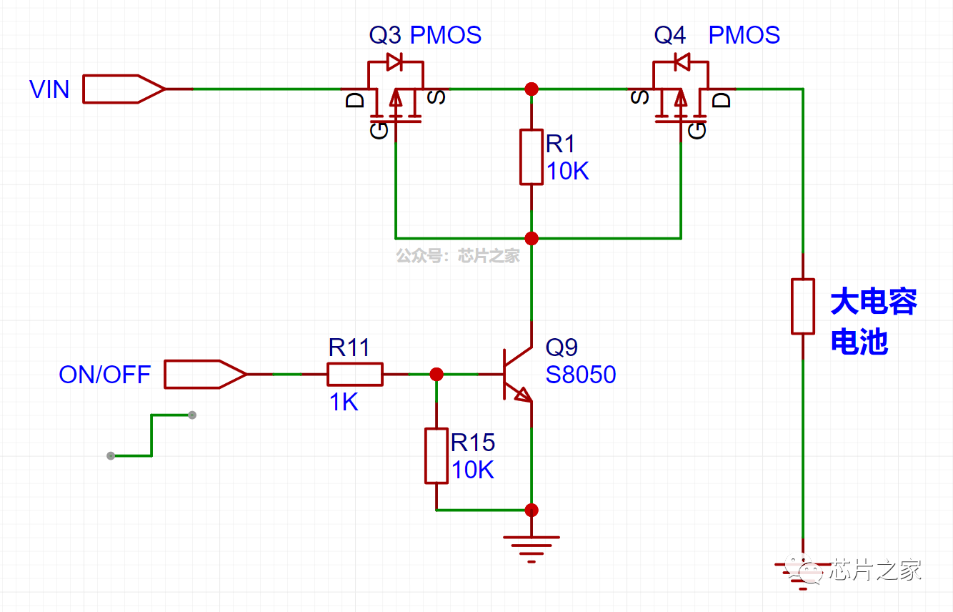
Let's take a look at the circuit above, which has an additional MOS. The two MOS are connected back-to-back. When the Control end ON/OFF is at a high level, the Q9 line of the transistor conducts, and the gates of Q3 and Q4 are pulled down to 0V. Q3 passes through the body diode, which meets the conditions for pilot conduction. Then, in Q4, the voltage at the S end is greater than the voltage at the G end, which also meets the conduction conditions. Conduction, the load end receives Vin voltage.
When the Control end is at low battery level, transistor Q9 is disconnected, Q3 and Q4 are not conducting, completely turned off, and the body diodes of Q3 and Q4 are in reverse series, so they are not connected in any direction, achieving the effect of preventing backflow.
The disadvantage of this circuit is that it still requires an IO to control, which is a bit cumbersome.
5. Double transistor mirror circuit anti backflow (ideal diode)
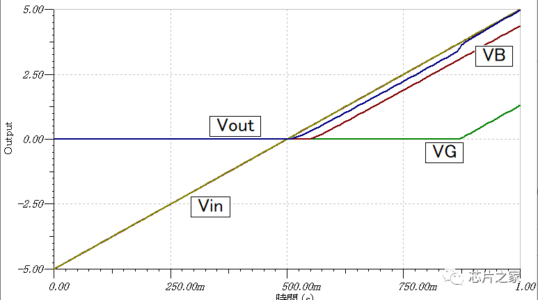
Circuit simulation results:
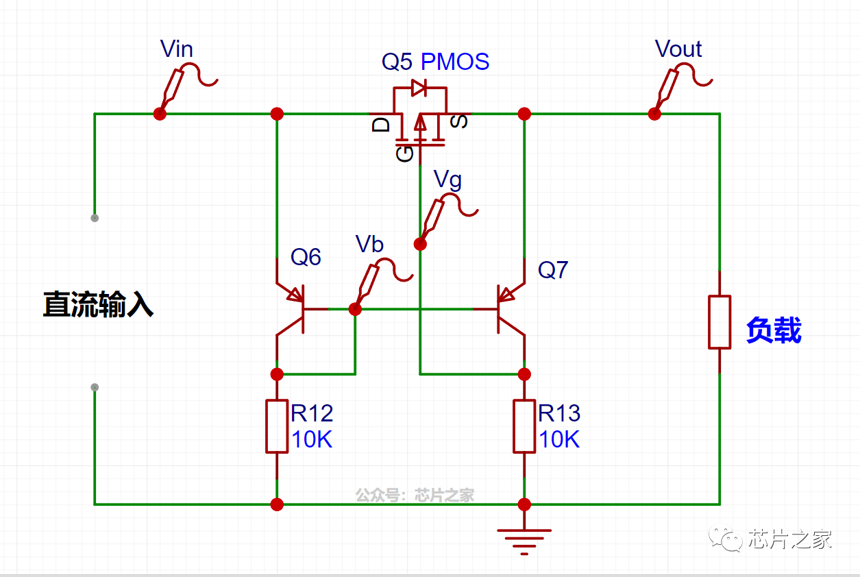
It looks like a mirror image, but it's actually not. How does this circuit work?
Left Q6 transistor, Vb=Vin-0.65, whether the right Q7 transistor is conductive is determined by Vb and Vout. If Vb>Vout-0.65, Q7 is turned off.
The above relationship has evolved into, Vin - 0.65 > Vout - 0.65, Then transistor Q7 is turned off;
If Vin>Vout, transistor Q7 is turned off;
When Vin inputs a certain voltage, Q6 saturates and conducts, and Q7 cuts off; The MOS transistor gate is grounded through a resistor and conducts;
If Vin is suddenly turned off, Vb is no longer constrained by the input voltage. At this time, Vb=Vout -0.65, Q7 conducts, the voltage at the G terminal of the MOSFET is pulled up, and the MOSFET is turned off, achieving the effect of preventing backflow.
Vin>Vout, MOS on, Vout ≈ Vin, ideal diode;
Vin<Vout, MOS turned off to prevent backflow.
The advantages of this circuit are anti reverse connection, minimal loss of voltage output, no need for additional control signals, and the ability to prevent current backflow.

