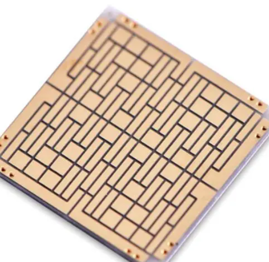
Asahi Chemical Corporation of Japan has successfully expanded the usable area of aluminum nitride substrates used in power semiconductors to 4.5 times that of previous mass-produced products. By using a substrate with a diameter of 4 inches (approximately 100 millimeters), the usable area can be expanded from 80% to 99%. The evaluation towards practicality has become possible, and we will start supplying samples to semiconductor manufacturers in the future, striving to achieve practicality as substrates by 2027.

Progress has been made in the research and development of materials such as silicon carbide (SiC) and gallium nitride (GaN) for the new generation of power semiconductors. However, among compound semiconductors, aluminum nitride has the highest resistance to high voltage, resulting in the lowest power loss. Practicalization requires achieving large caliber, and in 2023, it will be the first successful implementation of 4-inch technology worldwide. This time, the usable area has been increased from 80% to 99%, reaching a size that can be evaluated and verified for practicality.
The usable area has increased by 4.5 times compared to 2 inches of traditional mass-produced products, which helps to reduce costs. Previously, there were unusable parts on the edges of the substrate, but efforts were made to address temperature changes during the manufacturing process, making it 99% usable. In order to achieve practicality in the future, samples were provided to several semiconductor manufacturers. As a substrate, we strive to achieve usability before 2027 and install it on power semiconductor devices using aluminum nitride substrates around 2029.
It is expected to be first used for satellite communication and 5G base stations, taking advantage of its ability to cope with high frequencies. In the future, the plan is to further expand the caliber to 6 inches. Senior researcher Naoya Hisaishi stated that he plans to apply it to automotive applications such as chargers in the future.
Previously, Asahi Chemical has been using aluminum nitride substrates on deep ultraviolet LEDs for sterilization. This time, we will provide equipment manufacturing companies with substrates manufactured by our US subsidiary Crystal IS (New York State), which are expected to be used in next-generation power semiconductors and high-frequency equipment. The manufacturing cost will not vary significantly due to the size of the substrate, and the large-scale substrate will also help Asahi Chemical improve its profits.
In terms of substrates for next-generation power semiconductors, various chemical enterprises are promoting development and production enhancement. In terms of GaN substrates, Sumitomo Chemical of Japan has established a 4-inch mass production system and strives to achieve a 6-inch customer evaluation within the year. Mitsubishi Chemical Group has started supplying 4-inch samples. Resonac Holdings plans to enhance the domestic production capacity of SiC substrates in Japan after April 2027.
