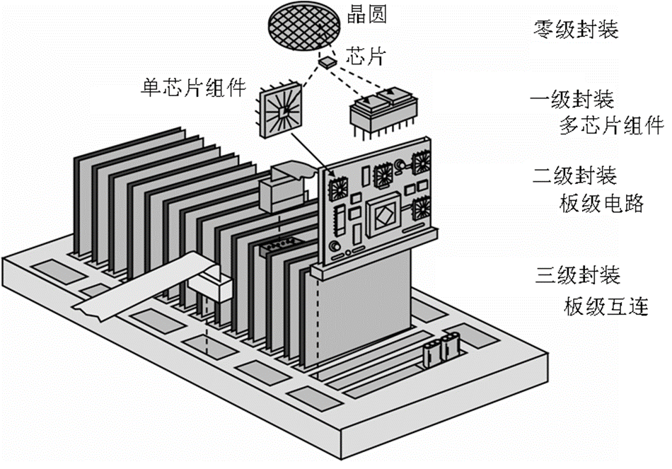
Many people understand chips, focusing mostly on process technology, wafer design, and core architecture, but often ignore the key link of chip packaging.
If wafer manufacturing is like building a "brain" for the chip, then packaging is like building a "bridge". Although they are all chips, some have long pins, some are smooth without pins, and some have many solder balls at the bottom. The main reason for these different appearances is different packaging processes. Today, Shunhai Technology takes you to understand common chip packaging.
First, understand the core issue: What exactly is chip packaging?
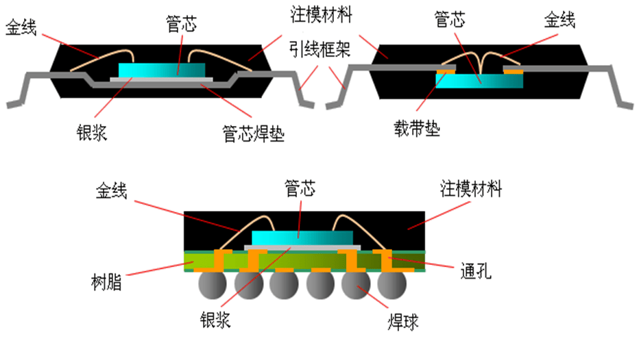
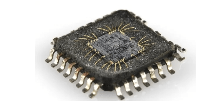
In simple terms, the bare chip cut from the wafer is very fragile and cannot be used directly. Chip packaging is the entire process of physical protection, electrical connection, and thermal optimization for the bare chip, making the originally exposed die into a finished chip that can be directly soldered onto a circuit board and work stably.
Depending on technical processes, pin arrangement, and application scenarios, we can divide all chip packages into five core categories, covering 99% of electronic device scenarios.
The role of packaging
1. Protection: Isolating the circuit working environment from the outside, with moisture-proof and dust-proof properties.
2. Support: The lead-out ends and housing maintain distance and buffer stress during assembly and welding.
3. Heat dissipation: Heat release when the circuit is working.
4. Electrical insulation: Ensuring no electrical interference with other components or circuit units.
5. Transition: Conversion of the physical size of the circuit.
Common chip packaging forms
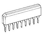
Through-hole mounting packaging: An old-fashioned basic model, simple and durable
This was the earliest form of chip packaging, with the biggest feature being long leads, which need to be passed through holes in the PCB board for fixation and welding.
The advantages are simple process, low cost, and convenient disassembly and maintenance; the disadvantages are large volume, high space consumption, and inability to meet the needs of miniaturized devices. It is currently only used for old-style, low-pin-count electronic devices.
Main subtypes:
1. DIP dual in-line package: The most classic old-style packaging, with pins arranged parallel on both sides of the chip, standard spacing of 2.54mm, easy to plug and unplug, strong compatibility. Early MCUs, logic chips, and many electronic beginners' first type of chip packaging were all this kind of packaging.

2. SIP single in-line package: The pins are concentrated on one side of the chip, arranged in a straight line, with a more simplified structure, often used for resistive networks, custom specialized chips, and other simple devices.
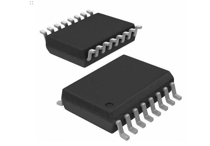
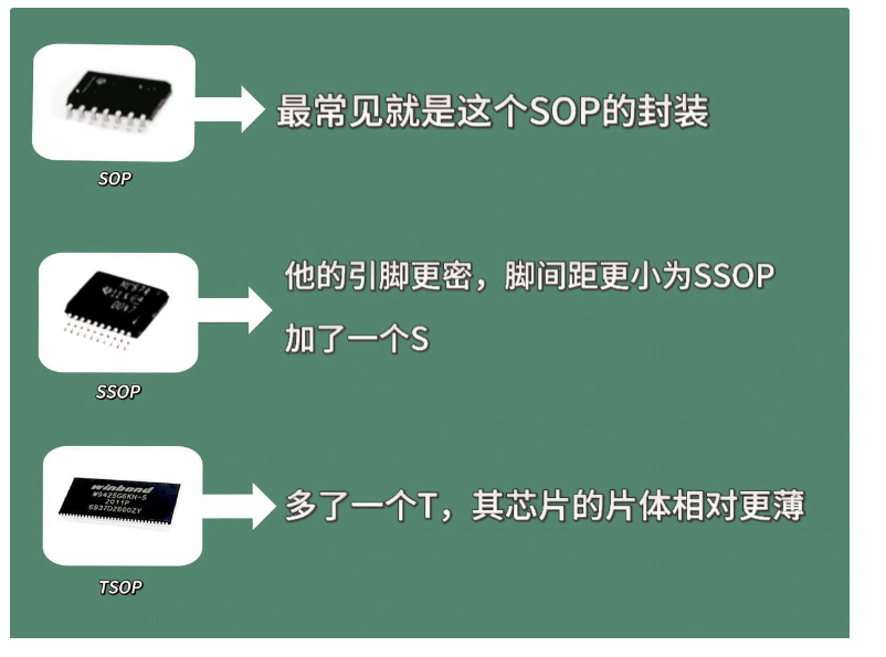
SMT surface mount packaging: The current mainstream consumer configuration
With the development of miniaturization of electronic products, through-hole packaging with long leads has been phased out, and SMT surface mount packaging has become the mainstream in consumer electronics.
No external long leads, the chip is directly soldered on the surface of the PCB board, smaller in size, higher pin density, and suitable for automated production. Most civilian chips in mobile phones, computers, and home appliances use this kind of packaging.
Main subtypes:
1. SOP standard plastic package: The chip has wing-shaped leads on both sides, which fit the circuit board for mounting. It has strong versatility and is widely used in conventional power chips, interface chips, and storage chips.
2. Narrow-body SOP/TSSOP ultra-thin narrow-body SOP: A compact upgrade of SOP, with narrower pins and thinner thickness, saving space significantly and specifically adapted for portable mini products such as earphones, bracelets, and small digital devices.
3. QFP quad flat package: The chip has fine wing-shaped leads on all four sides, with a large number of pins and high density, specially designed for complex function ICs. High-end MCUs, FPGAs, industrial control chips, and communication chips basically use this packaging.
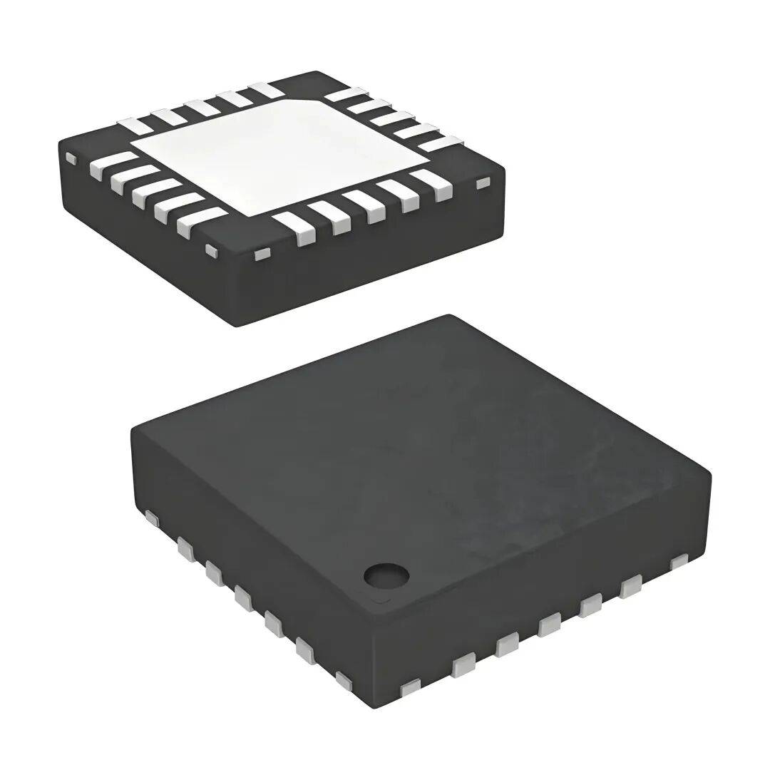
4. QFN/DFN leadless flat package: Eliminating external leads, it uses the bottom pad for electrical connection, with an extremely compact size and excellent heat dissipation performance, commonly used in smartphones, power management chips, and micro MCUs.
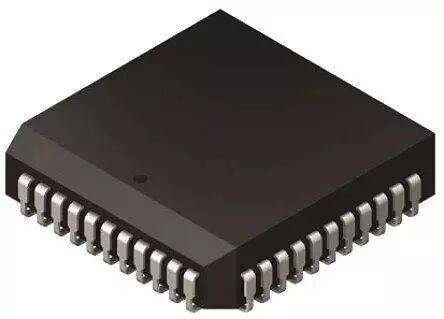
Array packaging: Exclusive for high-density high-end chips
For high-pin-count, high-performance high-end chips, conventional mounting packaging cannot meet the requirements, so array packaging was born. The core feature is that all contact points are concentrated at the bottom of the chip, significantly increasing the number of pins and electrical performance, suitable for high-end computing power and main control chips.
Main subtypes:
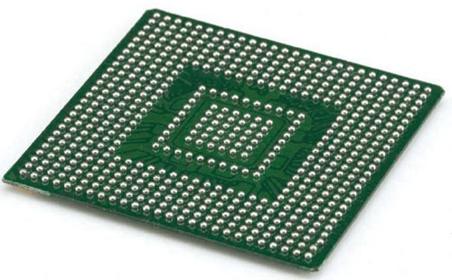
1. BGA ball grid array: The bottom of the chip is covered with a neat array of solder balls, with strong electrical transmission performance, good heat dissipation, and high stability. It is the standard packaging for computer CPUs, GPUs, high-end SoCs in mobile phones, and server chips.
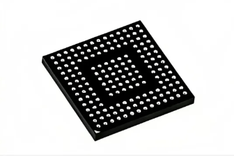
2. LGA land grid array: The bottom is a flat metal contact point, without solder balls or pins, and requires a dedicated socket for use. It is the exclusive packaging for Intel's high-end CPUs, with stable contact, high temperature resistance, and frequent disassembly and assembly capability.
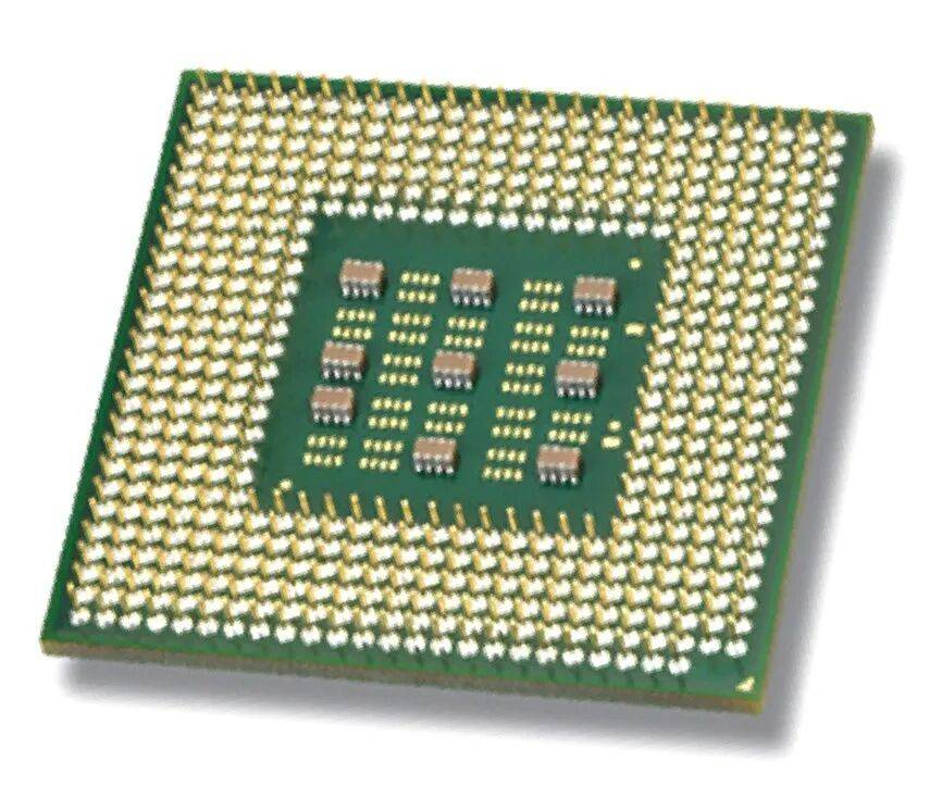
3. PGA pin grid array: The bottom has a metal pin structure. In the past, it was the mainstream CPU packaging form of AMD. It is easy to plug and unplug and has strong conductivity, but has been gradually upgraded and replaced.
Advanced high-end packaging: Core technology of the AI computing era
The boom of artificial intelligence, high-performance computing, and miniature intelligent devices has driven the iteration and upgrading of packaging technology. This kind of advanced packaging is no longer simply wrapping the leads, but rather achieving ultra-high integration, extreme miniaturization, and super performance through stacking, flip-chip, and wafer-level processes.
Main subtypes:
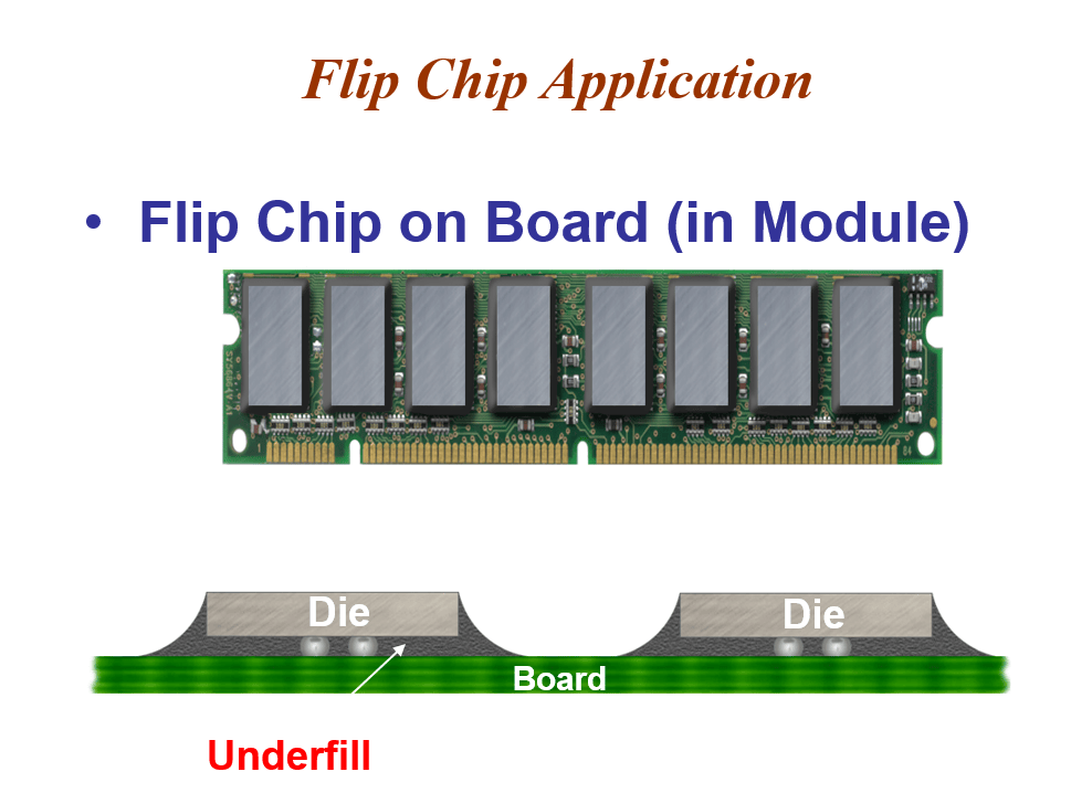
1. Flip Chip flip-chip: Breaking traditional top mounting processes, the chip is inverted and connected through micro bumps, with lower inductance and excellent high-frequency transmission performance, perfectly suitable for high-end processors, 5G RF chips, and other high-speed devices.
2. WLCSP wafer-level packaging: Complete the packaging on the entire wafer before cutting, with the finished product size almost the same as the bare chip, achieving the smallest packaging volume, widely used in mobile phone SoCs, micro sensors, and wearable device chips.
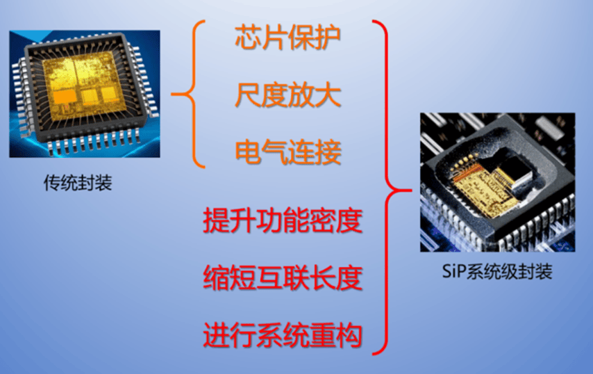
3. SiP system-in-package: Integrates multiple different functional bare chips and components into a single module, without complex motherboard wiring, significantly reducing the device size, and is the core packaging technology for mobile phone image modules, IoT chips, and smart wearable chips.
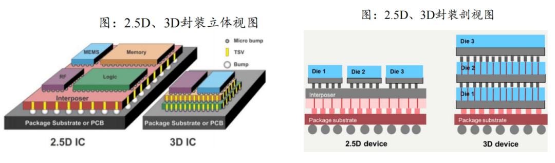
4. 2.5D/3D stacked packaging: Through silicon interposers and TSV vertical stacking technology, multiple chips are vertically stacked, greatly improving data transfer bandwidth and reducing latency, and is the core high-end packaging for AI GPUs, high-end HBM memory, and supercomputing chips.
Power devices & special packaging: Industrial power supply specific
Other than regular signal chips, industrial control, power equipment, and power devices require specialized packaging, focusing on heat dissipation, voltage resistance, and stability.
Main subtypes:
1. TO transistor packaging: Includes classic models such as TO-220 and TO-252, supporting both direct insertion and surface mounting, with built-in dedicated heat dissipation structures, with high voltage and high-temperature resistance, and is the mainstream packaging for MOSFETs, IGBTs, and voltage regulator chips, widely used in industrial control, home appliances, and power equipment.
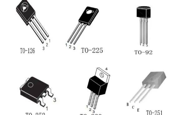
2. PLCC plastic J-lead carrier: Square structure, with J-shaped embedded leads on all four sides, high pin density, and a stable structure. It was commonly used for programmable logic devices (PLDs) and complex multi-pin ICs in the past, and is relatively common in older industrial control equipment.
Concluding remarks
From bulky glass and metal packaging to thin, precise BGA and CSP three-dimensional integrated packaging, the evolution of chip packaging is the history of the electronics industry becoming smaller, faster, more stable, and more energy-efficient. Packaging is not just about giving the chip a "clothes", but also a key core technology that determines the chip's heat dissipation, performance, stability, and adaptability to application scenarios.