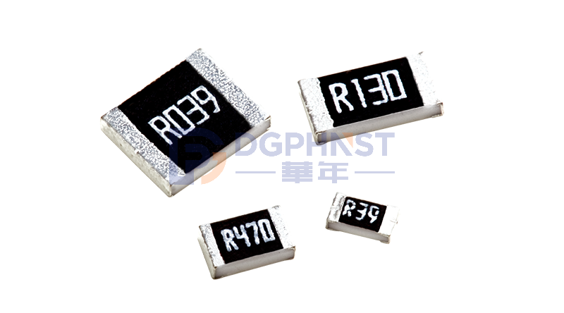
In previous articles, we have disassembled the internal structures of thick-film chip resistors and alloy resistors layer by layer (click blue text to view original: In-Depth Sharing | Layer-by-Layer Dissection of Thick-Film Chip Resistor Internal Structure, In-Depth Sharing | Dissection of Core Internal Structure of Alloy Resistors). This article will continue to explain the internal structure of thin-film chip resistors.
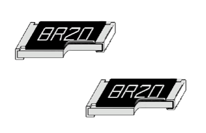
"Sandwich" Layer Structure
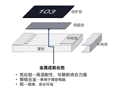
The thin-film chip resistor can be divided into external structure and internal core structure:
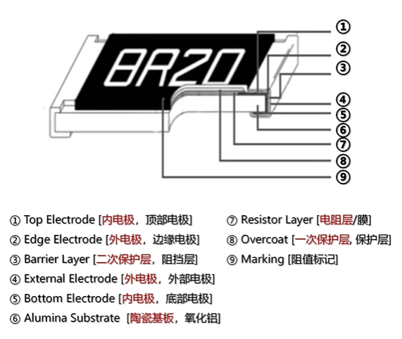
- External Structure (External Protection and Welding Terminal): Two outer-layer electrodes (three-layer composite welding structure) + overall encapsulation protective layer, connecting to the external circuit and isolating external damage.
- Internal Core Structure (Core Functional Body): Secondary protective layer + resistor film + internal electrode + ceramic substrate, determining resistance value accuracy, electrical performance, and service life.
Layer-by-Layer Dissection of Detailed Structure
Ceramic Substrate: The Foundation of Core Structure
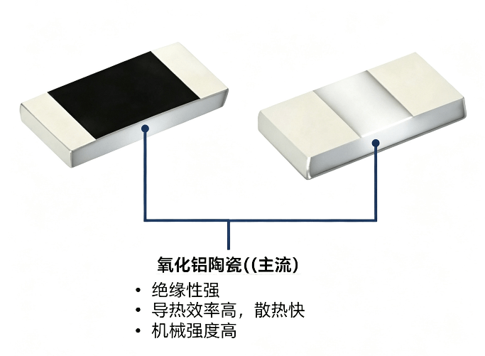
As the insulating base that carries all the core structures of the resistor, the substrate is the "foundation" of the entire resistor. Its strength, heat resistance, and insulation directly determine the basic stability of the resistor.
Main materials are aluminum oxide ceramic, used in most civil and industrial general applications. High-end materials like aluminum nitride ceramic are used in harsh environments such as aerospace, military, and precision medical fields.
Resistor Layer: The Core Structure Determining Resistance Value
This is the most core and critical functional layer of the thin-film resistor, and also the key to distinguishing high-end and low-end resistors. The resistance value, precision level, temperature coefficient, current-limiting and voltage-dividing capability are all determined by this layer.
Main materials: High-quality metals or metal oxides, including tantalum nitride, nichrome alloy, tantalum, etc. These materials are the core reason for achieving ultra-high precision of ±0.1%, ±0.05%.
First Protective Layer: Initial Protective Function
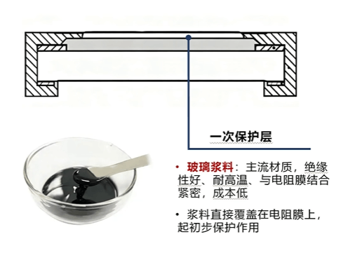
The resistor layer is precise and fragile, and during subsequent laser trimming, plating, and cleaning processes, it is easily eroded by chemical solutions, contaminated by impurities, or damaged mechanically. The first protective layer is designed to solve this problem.
Core function: Fully encloses the resistor film and laser trimming groove, isolating plating solution, processing impurities, and external ion pollution.
Common materials: High-purity glass paste.
Second Protective Layer: Ultimate Protective Function
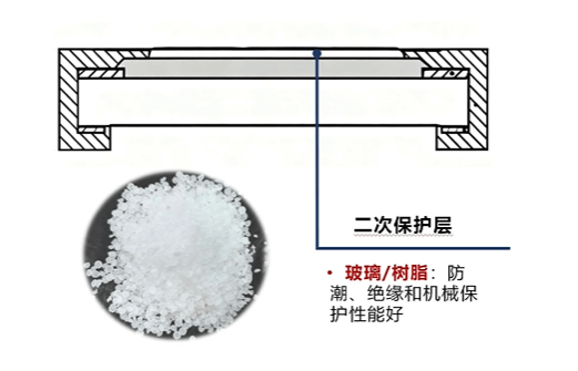
Core function: Fully seals the core body of the resistor, isolating moisture, oxygen, acidic and alkaline chemicals, dust, and other external interferences from the air.
Common materials: Glass and resin, offering strong moisture resistance, insulation, and mechanical compression resistance.
Terminal Electrode Layer: Connection to External Circuit
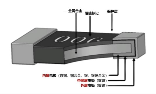
The terminal electrode connects the resistor to the external PCB circuit and achieves conduction. It adopts a three-layer composite structure:
- Inner Layer (Bonding Layer): Made of copper alloy or silver-palladium alloy, with excellent conductivity and strong adhesion to the ceramic substrate and resistor film layer, preventing electrode detachment and poor contact issues.
- Middle Layer (Barrier Layer): Common material is nickel, which serves as a "diffusion barrier." It effectively prevents the internal silver material and external solder material from diffusing into each other during high-temperature soldering, avoiding electrode corrosion and performance failure.
- Outer Layer (Soldering Layer): Common material is tin, with excellent solderability, compatible with conventional reflow soldering and wave soldering processes, easy to solder, with full solder joints and less risk of false soldering or desoldering.
Final Words
A small thin-film chip resistor has become the "standard component" of high-end circuits due to its compact size, high precision, and low temperature drift. From the base support, resistor film preparation, dual-layer protection packaging, to the electrode conduction path, the internal structure is layered and clearly defined, ensuring the performance and long-term stable operation of the resistor.