Driven by faster connection speeds, higher levels of automation, and smarter systems, Industry 4.0 has accelerated the application of visual technology in the manufacturing industry and introduced intelligence into previous simple data acquisition systems. The previous generation of visual systems was responsible for capturing images, encapsulating them for transmission, and providing image data for processing in subsequent FPGA, ASIC, or expensive SoC devices. Nowadays, Industry 5.0 goes further by integrating artificial intelligence (AI) and machine learning (ML) into the entire data path, achieving large-scale customization. Cameras have become intelligent, capable of processing image data at the application level and only outputting metadata for decision-making.
The key development between these two generations is to focus on the changes that occur at the edge. Our world is essentially simulation driven, and many electronic and electromechanical (EEM) systems that help us with our daily lives are driven by various perceptual inputs. Electronic sensors at the edge of the system, such as visual (light), temperature (heat), audio (sound), distance and position, and pressure (tactile), collect these physical inputs and convert them into processed data to achieve intelligence and facilitate decision-making.
Industry 4.0 has put forward a demand for intelligent and efficient sensors of this type. Nowadays, numerous sensors in non industrial and commercial applications are constantly evolving, from basic types to enhanced versions that comply with industrial automation processes and standards.
Along with the large-scale adoption of sensors, people are also promoting the widespread application of lower power battery driven intelligent devices. Power consumption poses different challenges to the visual system, and how image sensors can solve these challenges in innovative ways while providing excellent performance will become a differentiating factor in the visual system.
Image Sensor - Input Mechanism of Visual Perception
Visual perception has become one of the important ways to collect data at the edge, and the collected image data can be quickly and efficiently used for decision-making. For example, without visual sensors, objects in the scene require countless specific sensors to convey the composition of the scene. This will generate a large amount of data and require extensive processing work, perhaps relying on good luck to obtain a realistic presentation of the scene. In addition, in an efficient system, one image can convey all the information in the scene in one frame of data.
This simple form of data representation enables the accelerated development of image sensors, providing support for consumer mobile products such as smartphones, with a resolution of over 100 million pixels. With hardware and software support, it provides excellent detail features for static images and video streams. Due to the fact that mobile products mainly serve entertainment and personal applications, their decision-making goals are slightly different. However, visual systems for automotive, industrial, and commercial applications serve highly goal oriented needs, many of which use (sensor) outputs for machine based decision-making and require a fine balance between resolution, frame rate, and power consumption.
With the increasing importance of edge intelligence, these applications must adapt to different use case requirements. Nowadays, many applications require higher resolution and better overall performance to assist computer vision, machine vision, and automation decision-making systems.
In many cases, people are very eager to obtain richer details because these details help reduce erroneous decisions. As the resolution increases, the number of pixels in the image sensor also increases, and correspondingly, the amount of image data provided by the sensor to the Image Signal Processor (ISP) or System On Chip (SoC) also increases. The large amount of image data generated by sensors and the processing of these data by ISP/SoC can lead to high power consumption, thus placing a huge burden on visual system design.

Figure 1: The data generated by the image sensor increases exponentially with resolution and frame rate
Now, designers need to deal with issues such as high-power transmission, power consumption, and system bill of materials (BOM) costs brought about by high-power electronic components. Although reducing power consumption is the trend, thermal management is also a challenge, as most visual systems rely on convective airflow to dissipate the heat generated in the system. Image sensors are highly sensitive to heat, and if appropriate design and effective management of these factors are not chosen, unreliable visual systems can arise.
Everything starts with quantum efficiency
The quantum efficiency (QE) of an image sensor refers to the ability of a photodiode to convert incident photons into electrons to the maximum extent possible. As is well known, the higher the QE, the better the brightness of the image. Higher QE values are crucial in low light conditions, typically achieved by using larger pixel sizes or adding visible or invisible light to the scene. Regardless of the method, it will increase the cost, power consumption, and space that the visual system must support, and may grow exponentially based on the performance of image sensors and scene conditions.
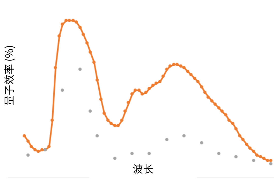
Figure 2 Normalized quantum efficiency curves of comparable pixel sizes at different wavelengths
This is particularly severe in invisible lighting situations where infrared light-emitting diodes (IR LEDs) are commonly used, producing light wavelengths of 850nm and 940nm. These wavelengths can be detected by image sensors, but cannot be detected by the human eye. In the industry, this is commonly referred to as "active lighting". Infrared light-emitting diodes require power supply and generate power consumption, occupying a large amount of space and significantly increasing the system BOM cost. Image sensors with high quantum efficiency in near-infrared spectroscopy can reduce their usage, light intensity, and overall BOM cost without sacrificing image quality.
Higher image quality and lower overall cost of ownership
It is important to ensure that the high QE provided by image sensor pixels is not affected by noise from other parts of the data path, thereby affecting the overall image quality. For example, if the pixel structure does not have sufficient pixel spacing, pixel to pixel crosstalk will reduce the modulation transfer function (MTF) and contrast/clarity of the image, ultimately affecting image quality. Another possible factor that can cause damage is the high reading noise caused by poor performance of the readout circuit.
Poor image quality can bring unnecessary burden to ISP/SoC, requiring it to process more data, thereby reducing the overall frame rate of the visual system, or running at higher clock frequencies to maintain the same end-to-end timing. In the former case, the efficiency of the visual system will be greatly reduced, and in either case, the system will ultimately generate more power consumption. To cope with the processing burden, it may be necessary to equip ISP/SoC with more advanced resources, which will further increase the overall BOM cost. Excellent image output quality can alleviate the aforementioned shortcomings and reduce the overall cost of ownership of the visual system.
Subsampling mode
Ansemy's image sensors (such as the HyperluxTM LP product line) have recognized these operational requirements and integrated multiple seed sampling modes. These modes, such as Binning, Cropping, and Skipping, can greatly reduce the bandwidth required for generation and transmission.
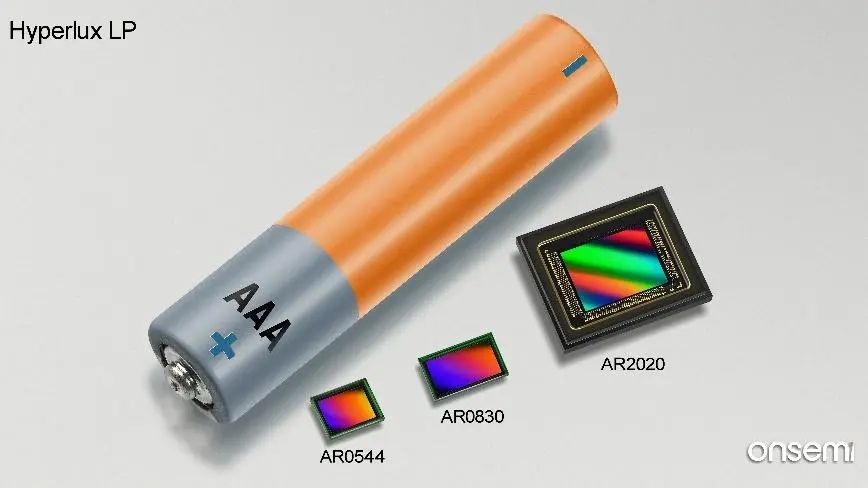
Figure 3 Ansemy Hyperlux LP Series Products
These features make the visual system very intelligent, capable of selecting the optimal power consumption/performance configuration based on use case requirements. For example, in biometric scanners, a single system equipped with a 5-megapixel sensor array can now be used to gradually enhance scanning from a single fingerprint in sub sampling mode to a full resolution facial scan. The most important thing is that the amount of data received by ISP/SoC is reduced, thereby reducing the power consumption of itself and the entire visual system.
Reduce data size
High resolution image sensors consume a significant amount of bandwidth to output data. For example, a 20 million pixel sensor operating at a speed of 60 frames per second will transmit 12 Gbps image data, which not only needs to be properly processed in the high-speed interface inside the sensor, but also needs to be processed by the ISP/SoC that receives this data. Processing such a large amount of data requires expensive and dedicated resources and power investment in these processing engines, which may lead to significant power consumption/thermal management issues. In addition, the limitation of interface speed has also increased this challenge.
In most applications, only a small portion of the time may be required to run at full speed at full resolution, while the rest of the time only requires lower resolution. Although subsampling mode can reduce bandwidth and has its own advantages, it is limited in terms of resolution selection or scene integrity.
The scaler inside the sensor helps to overcome these limitations and effectively meet the needs of low resolution operations. They can control bandwidth at the source, rather than being managed by ISP/SoC. They can provide precise granularity control to the maximum extent while maintaining a complete field of view (FOV).
The image scaling algorithm of the Ansemy AR2020 image sensor (a 20 million pixel member of the Hyperlux LP product series) is very complex, providing excellent image quality even in cases of significant resolution scaling. For example, although obtaining details of distant objects does require 20 million pixels, it may only require a specific area of the image, not the entire image. By cropping or scaling this dynamically defined area, the advantage of a 20 million pixel sensor can be achieved without the need for continuous processing of data equivalent to 20 million pixels.
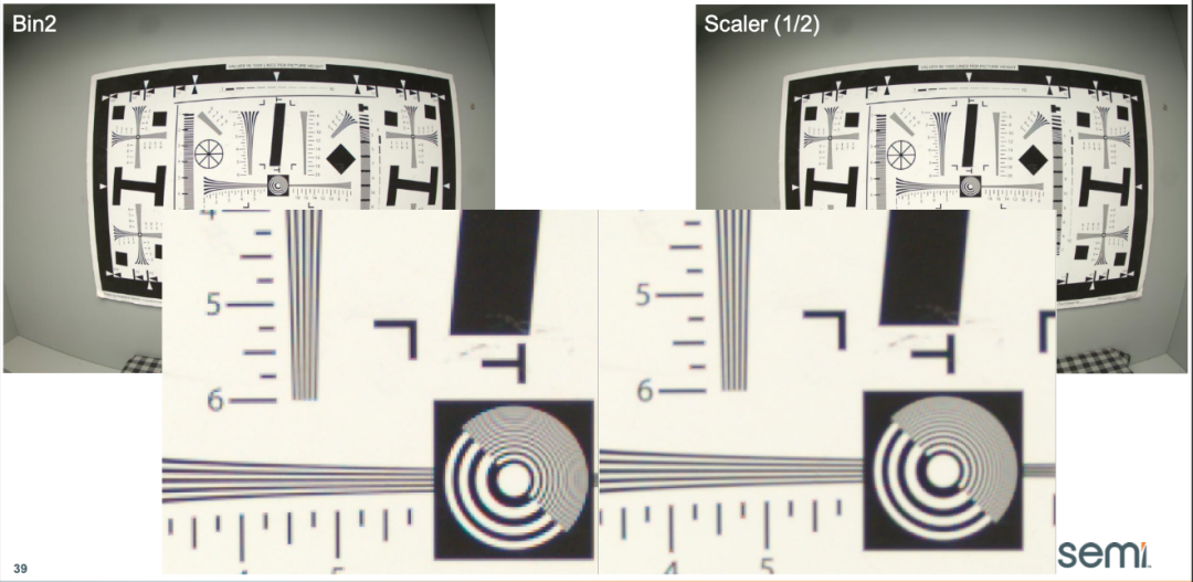
Figure 4: Scaling produces fewer artifacts than binning, thereby improving the image output effect
Sleep as much as possible and wake up as needed
Sensors can operate at extremely low resolutions and the lowest frame rate during most working hours. When motion is detected, it switches to the predetermined configuration - Wake up to Motion (WOM) mode. The image sensor has the ability to handle these changes and have the ISP/SoC switch it to the desired mode/configuration. It can further shield motion areas unrelated to the application, making sensors and visual systems more precise and efficient. Previously, this feature was completed in the processor, but implementing it on sensors can reduce system resources and power consumption.
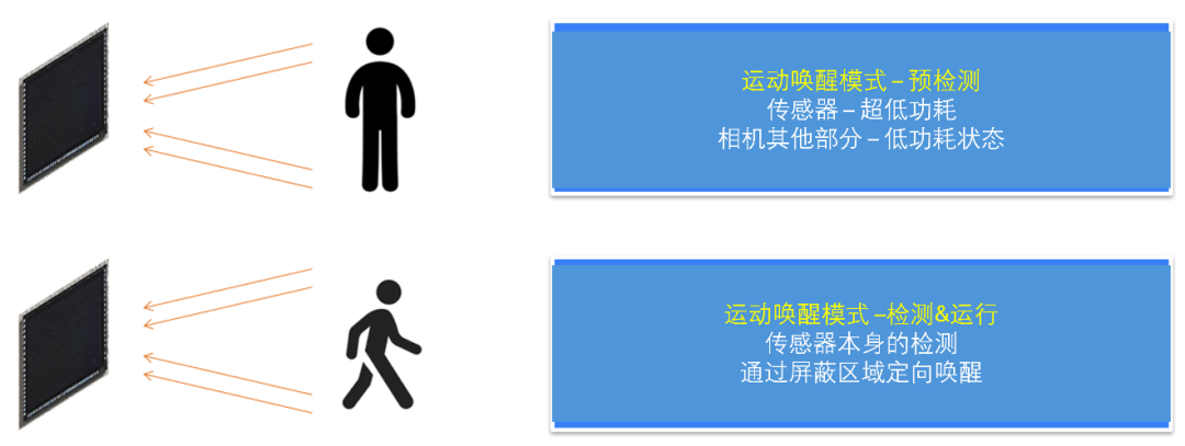
Figure 5. Functions such as motion wake-up give the visual system a high degree of target drive
We can see the profound impact of these features in battery powered applications, intelligent access control systems, retail scanners, medical monitoring systems, and similar applications. Battery powered applications benefit the most from these sensors as they can minimize system power consumption.
In the 4K video doorbell application, 8-megapixel image sensors like the Ansemy AR0830 transmit 6G of data at full load, but now it can run for over 98% of its working time in WOM mode. In the pre detection stage, the amount of data generated/transmitted is extremely low, and the operating power consumption of the entire visual system is only a small part of that in full working mode.
So far, image sensors have performed excellently as data capture and transmission devices. As demonstrated in the Ansemy Hyperlux LP product line, the above trends and advancements make these sensors powerful edge devices for built-in intelligent applications. By integrating better pixel technology, configurable intelligent focus areas, motion detection and other functions, it can now be designed to meet specific use case requirements, thereby creating high-performance and low-power differentiated and efficient visual systems.


