The Hidden Bottleneck in the Competition of High-End Chip Computing Power
When it comes to domestic high-end chips and computing power competitions, most people focus on core chips such as GPU, CPU, and AI large computing processors. Few people realize that the bottleneck restricting the performance ceiling of high-end computing chips is not computing power itself, but unstable chip power supply.
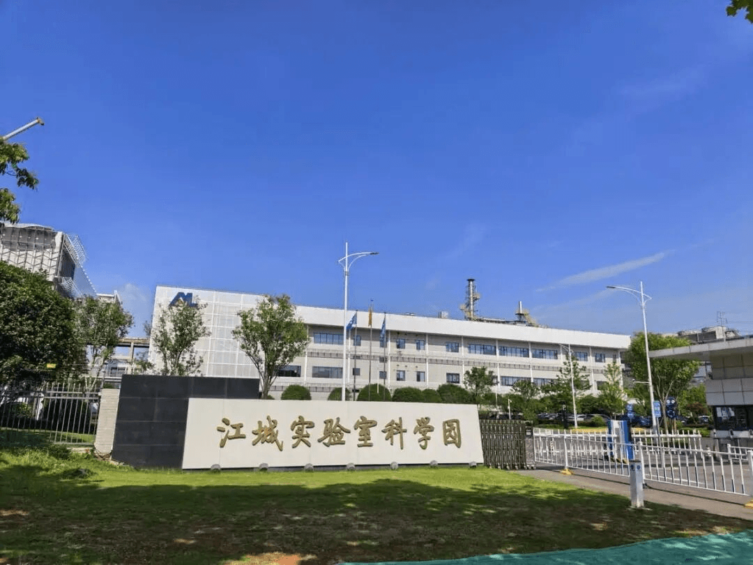
Major Breakthrough by the Jiangcheng Laboratory in Hubei
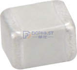
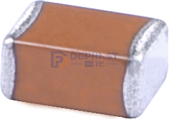
Recently, the Jiangcheng Laboratory in Hubei has made a major breakthrough in capacitor key technology! It independently developed a three-dimensional multi-layer on-chip capacitor with a capacitance density exceeding 1000 nF/mm², specifically designed for high-end AI/GPU and high-performance processors, supporting the development of high-computing power, low-power chips.
The Key Constraint for AI Chip Performance: Power Imbalance
Many people don't understand: Why can a small capacitor restrict the performance of top-tier GPUs and AI processors?
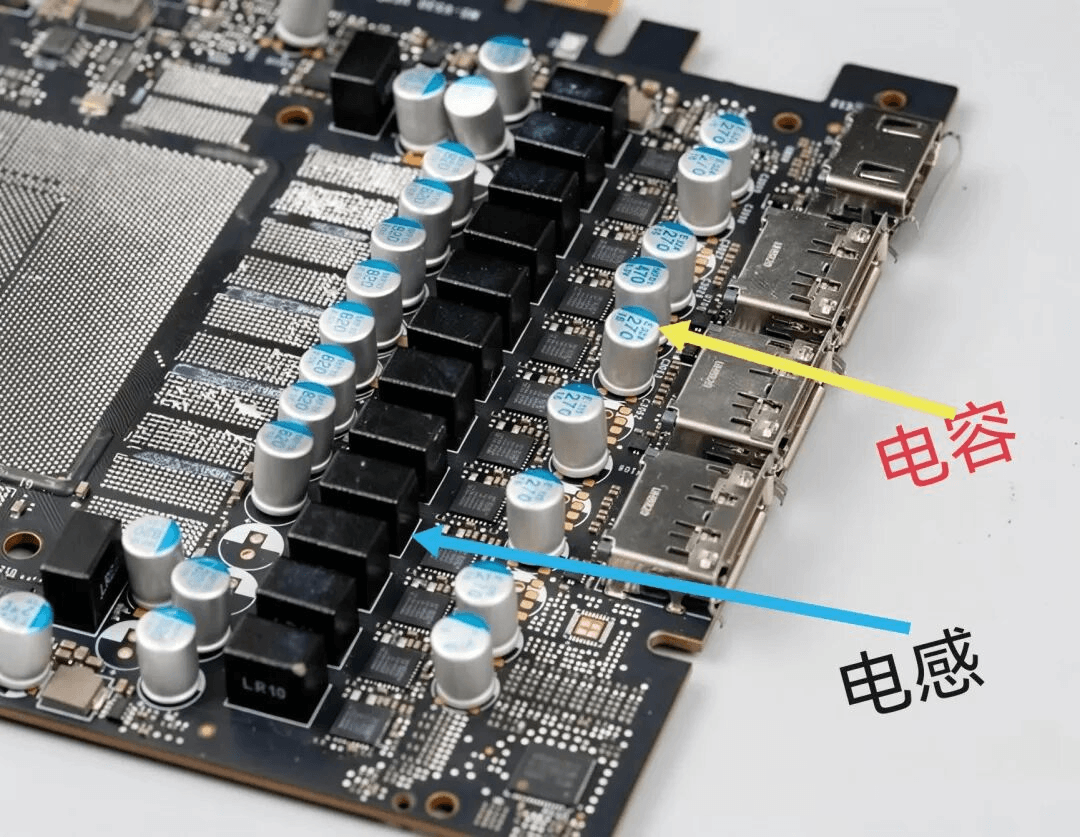
In simple terms, capacitors act like mini water reservoirs in circuits. When there are significant fluctuations in chip current, they quickly charge and discharge to stabilize voltage, delivering stable and clean current to the chip. In computing systems, capacitors are referred to as "electric RAM": HBM handles data buffering, while capacitors handle energy buffering. When a GPU runs at full load with high power, it relies on multi-stage capacitor energy storage, operating at nanosecond to second level, to ensure sufficient and stable power supply.
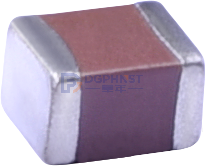
Traditional off-chip MLCC and electrolytic capacitors are far from the chip core, have slow response times (microsecond/millisecond level), and their capacitance density is generally less than 20nF/mm². Under severe voltage disturbances, the chip can only actively reduce frequency to protect itself, directly leading to lagging during large model training, reduced computing power, and overheating or system crashes.
In short: traditional capacitors either respond too slowly or take up too much space; even the best domestic GPU and AI chip architectures cannot fully utilize their native computing power.
The Emergence of Silicon-Based Three-Dimensional Multi-Layer Capacitors, Performance Surpasses by Hundreds of Times
According to official disclosures from the Jiangcheng Laboratory, the three-dimensional through-hole capacitor based on silicon dioxide dielectric material completely discards traditional design concepts, using mature silicon-based processes. It etches micrometer-level deep holes in silicon wafers, depositing high dielectric constant materials and metal electrodes alternately on the hole walls, similar to upgrading thin paper into a high-density energy storage sponge. The energy storage capacity under the same area increases by hundreds of times.
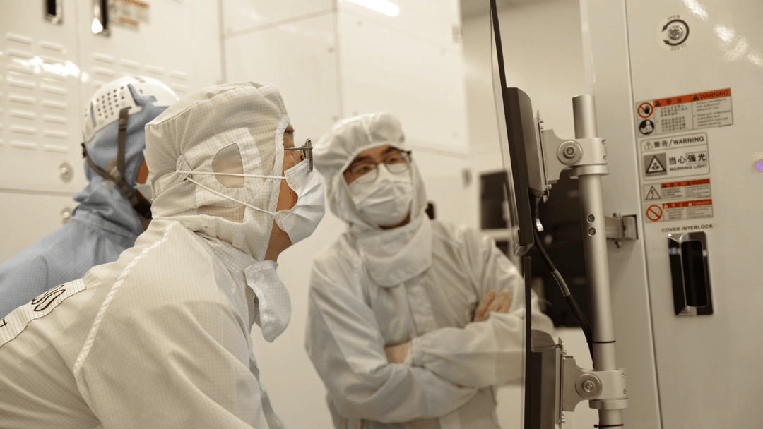
Engineers at the Jiangcheng Laboratory are analyzing experimental data on an advanced packaging integrated test platform
Key Benchmark Parameters
Capacitance density exceeds 1000nF/mm² (1μF/mm²); compared to traditional planar MIM capacitors (10-80nF/mm²), its performance improves by more than 100 times, and its voltage stabilization capability is hundreds of times better than conventional MLCC laminated ceramic capacitors;
Full-Chain Independent Breakthrough
For a long time, high-end on-chip capacitors and related advanced packaging technologies have been controlled by overseas industry giants. Many domestic chips, even if their architecture and computing power parameters match international top standards, are constrained by shortcomings in power components, making it difficult to run at full load and high frequency stably.
The R&D team at the Jiangcheng Laboratory independently developed a dedicated analysis model, first incorporating the effects of coaxial transmission through holes and high-frequency dynamic characteristics, simplifying complex electromagnetic simulations into algebraic equations, increasing computational efficiency by hundreds of times. Each simulation takes only a few minutes, and compared to traditional high-precision simulation results, the maximum overall error is controlled within 5%.
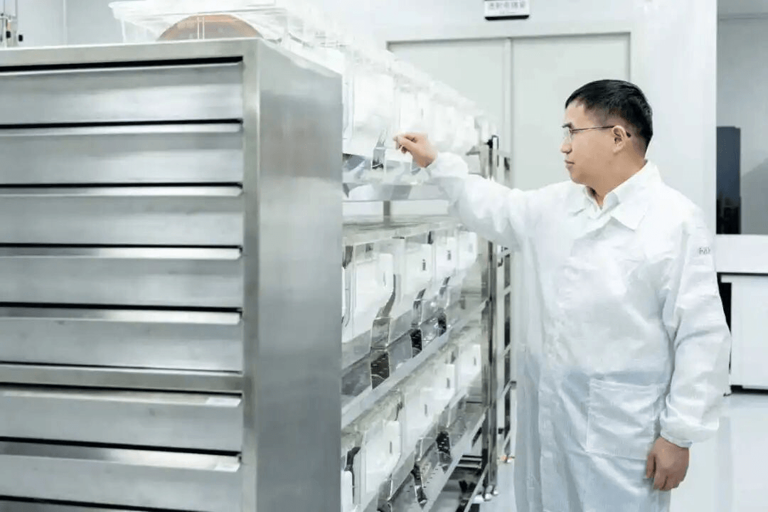
Director Yang Daohong of the Jiangcheng Laboratory working
This technological breakthrough has achieved full-chain self-control in materials, structures, processes, and modeling, completely breaking through overseas process and IP barriers, and addressing the shortage in China's high-end chip passive component field.
Clear Industrialization Progress
Currently, 2.5D/3D advanced packaging has become a standard for high-end computing power, and on-chip integrated capacitors are a core component of the interposer.
The Jiangcheng Laboratory completed compatibility verification using a 12-inch advanced packaging test platform. After the technology is mass-produced, domestic packaging and testing plants, as well as chip design companies, will no longer need to purchase expensive overseas capacitor IP and manufacturing services, simultaneously improving the cost and autonomy rate of the entire advanced packaging industry chain.
In Conclusion
According to the laboratory's industrialization plan, after completing small-batch trial production and optimizing yield, mass production is expected to be achieved within one year, primarily supplying domestic leading AI chips and advanced packaging companies. In addition to AI/GPU, this three-dimensional capacitor structure can also be adapted to high-integration, high-instantaneous power consumption scenarios such as high-speed optical modules, 5G RF, and automotive-grade high-performance processors.
From an industrial cycle perspective, although passive components seem small, they are the cornerstone of the independent control of integrated circuits. Following the breakthroughs in high-end resistors and special MLCCs, the ultra-high-density on-chip capacitor has achieved another milestone. China's electronic components are now comprehensively permeating into high-end chip-level support, continuously reinforcing the foundation of underlying hardware.
Do you think that the first beneficiaries of this capacitor's mass production will be the chip design end or the packaging and testing sector? Please leave your comments in the comment section.