With Intel, Samsung, TSMC, and Japan's upcoming advanced wafer foundry Rapidus, although each company is preparing to pack more and more transistors into each square millimeter of silicon wafer, they have one thing in common: the extremely complex and expensive EUV lithography technology they rely on, as well as extremely high operating costs. The main reason is that the 13.5 nanometer light source of the system is the precise and expensive process of using the most powerful commercial laser on Earth to spray scattered molten tin droplets.
But an unconventional alternative solution is brewing. A group of researchers from the Tsukuba High Energy Accelerator Research Organization (KEK) in Japan believe that if the energy of particle accelerators is utilized, EUV lithography technology may be cheaper, faster, and more efficient.
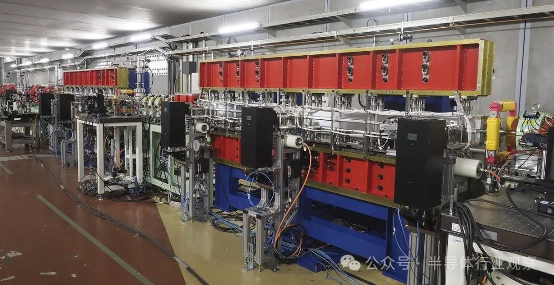
Even before the installation of the first batch of EUV machines in wafer factories, researchers saw the possibility of using powerful light sources generated by particle accelerators (free electron lasers) for EUV lithography. However, KEK scientists suggest that not any particle accelerator can achieve this. They claim that the best candidate for EUV lithography is to use the particle accelerator version of regenerative braking. It is called an energy recovery linear accelerator, which can economically generate tens of kilowatts of EUV power for free electron lasers. This is enough to drive more than one but multiple next-generation lithography machines simultaneously, thereby reducing the cost of advanced chip manufacturing.
KEK Advanced Light Source Researcher Norio Nakamura told me during a visit to the facility, "The extremely high power, narrow spectral width, and other characteristics of FEL beams make them very suitable for future lithography technologies."
Linear Accelerator and Laser Plasma
The current EUV system is manufactured by only one manufacturer, ASML, headquartered in Feldhofen, Netherlands. When ASML launched its first generation of precision machines worth over $100 million in 2016, the industry's demand for them was very urgent. Chip manufacturers have been trying various alternative methods to cope with the most advanced system at the time, which was the photolithography technology using 193 nanometer light. Turning to shorter wavelengths of 13.5 nanometers is a revolution that will reduce the number of steps required for chip manufacturing and keep Moore's Law valid for the next decade.
The main reason for sustained delay is that the light source is too dim. The technology that can ultimately provide sufficiently bright EUV light sources is called laser plasma (EUV-LPP). It uses a carbon dioxide laser to spray molten tin droplets into plasma thousands of times per second. The plasma emits a photon energy spectrum, and then specialized optical devices capture the necessary 13.5 nanometer wavelength from the spectrum and guide it through a series of mirrors.
Subsequently, EUV light is reflected off the patterned mask and projected onto the silicon chip.
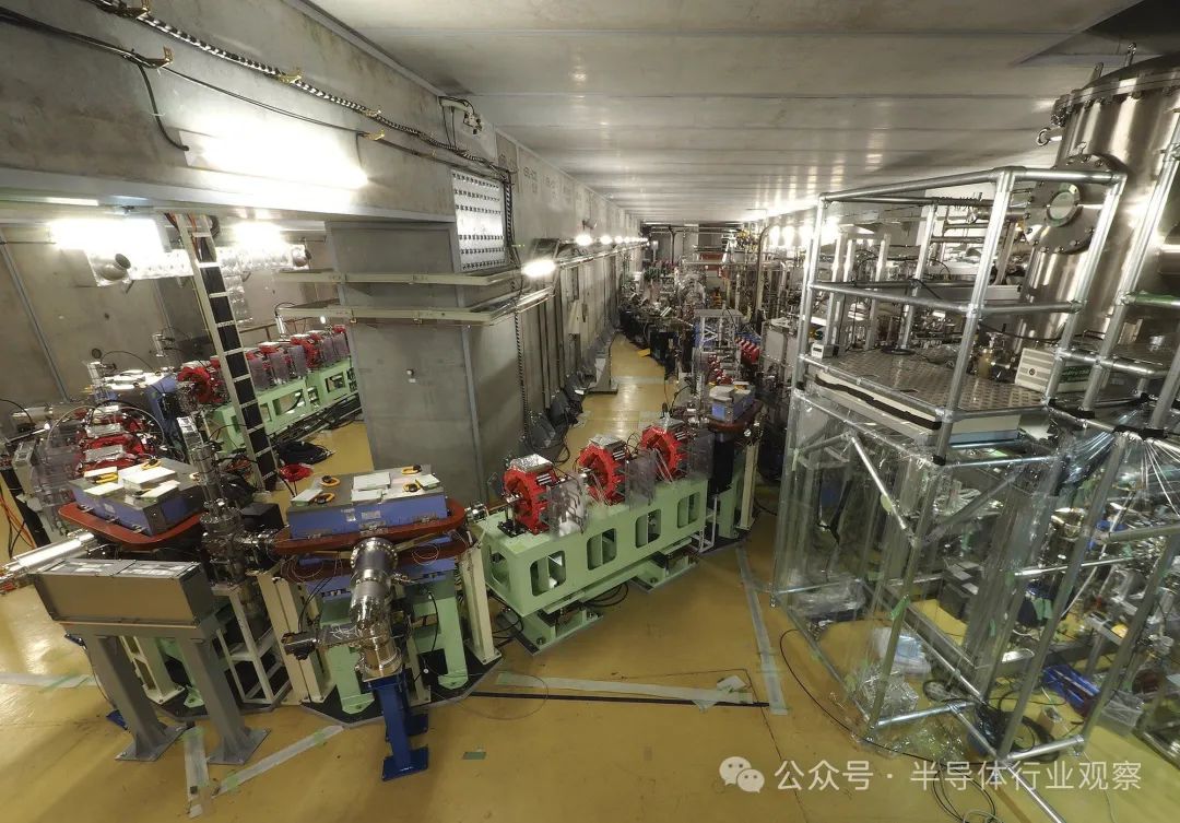
KEK's experimental compact energy recovery linear accelerator utilizes most of the energy from the electron return process to accelerate a new set of electrons
All of these add up to a highly complex process. Although it started with a laser that consumed up to kilowatts of electricity, the amount of EUV light reflected onto the wafer was only a few watts. The darker the light, the longer it takes to reliably expose the pattern on the silicon wafer. If there are not enough photons carrying patterns, the speed of EUV will be uneconomical. Overly pursuing speed may lead to costly mistakes.
When the machine was first launched, the power level was sufficient to process about 100 wafers per hour. Since then, ASML has successfully steadily increased the production of the current series of machines to around 200 wafers per hour.
The current rated power of ASML light sources is 500 watts. But Nakamura said that in the future, more refined patterns are needed, which may require 1 kilowatt or higher power. ASML states that it has a roadmap for developing 1000 watt light sources. But this may be difficult to achieve, according to Nakamura, who previously led KEK's beam dynamics and magnet team and resumed working on EUV projects after retirement.
It's difficult, but it's not impossible. Ahmed Hassanein, director of the Center for Materials Research in Extreme Environments at Purdue University in Indiana, said doubling the power of light sources is "very challenging". But he pointed out that ASML has achieved similar high difficulty goals in the past through a comprehensive approach of improving and optimizing light sources and other components, and he does not rule out the possibility of repeating this approach.
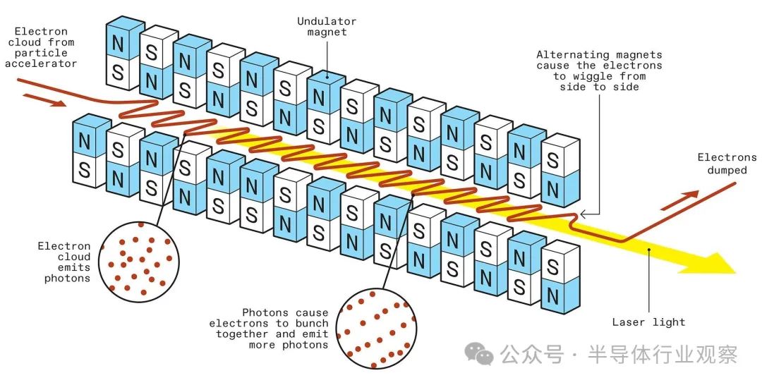
In a free electron laser, accelerating electrons are affected by an alternating magnetic field, causing them to fluctuate and emit electromagnetic radiation. Radiation gathers electrons together, causing them to only amplify specific wavelengths, thus producing a laser beam.
But brightness is not the only problem ASML faces in terms of laser plasma sources. "There are many challenging issues when upgrading to higher EUV power," Hassanein said. He listed several issues, including "pollution, wavelength purity, and performance of mirror collection systems."
Another issue is the high operating costs. These systems consume approximately 600 liters of hydrogen gas per minute, most of which is used to prevent tin and other pollutants from entering optical components and wafers. (However, recycling can lower this number.)
But ultimately, operating costs still depend on electricity consumption. Stephen Benson, a retired senior researcher at Thomas Jefferson National Accelerator Facility in Virginia, estimates that the electro-optical conversion efficiency of the entire EUV-LPP system may be less than 0.1%. He said that the efficiency of the free electron laser being developed by KEK may be 10 to 100 times higher than the former.
Energy recovery linear accelerator
The system being developed by KEK generates light by accelerating electrons to relativistic velocity and then deviating from their motion in a specific way.
Nakamura explained that this process begins with an electron gun injecting an electron beam into a several meter long low-temperature cooling tube. In this tube, superconductors emit radio frequency (RF) signals, driving electrons to move faster and faster. Then the electrons rotate 180 degrees and enter a structure called a oscillator, which is a series of magnets with opposite directions. There are currently two KEK systems. The oscillator forces high-speed electrons to move along a sinusoidal path, which causes electrons to emit light.
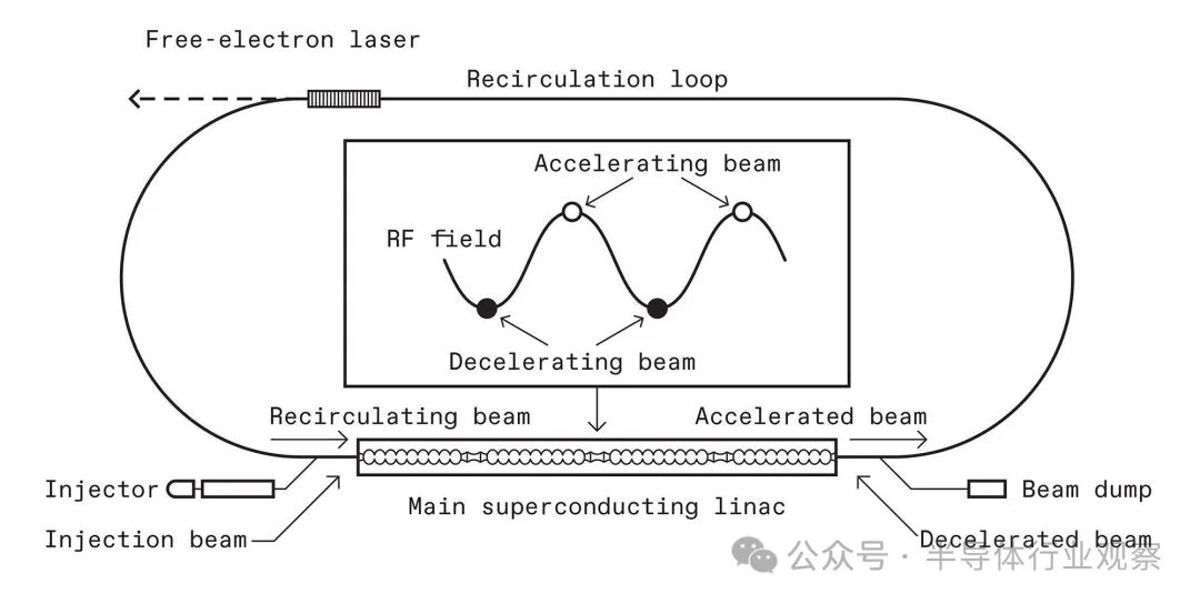
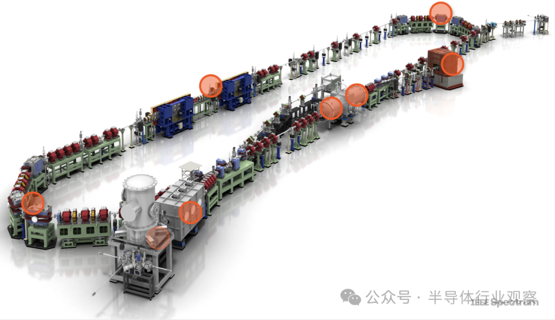
In a linear accelerator, the injected electrons obtain energy from the radio frequency field. Usually, electrons then enter the free electron laser and are immediately processed into the beam collector. But in an energy recovery linear accelerator (ERL), electrons return to the radio frequency field and lend their energy to newly injected electrons before entering the beam collector. (Detailed explanation attached at the end of the text)
The phenomenon that occurs next is called self amplified spontaneous emission (SASE). The interaction between light and electrons slows down the speed of some electrons and accelerates the speed of others, resulting in their aggregation into "microbeams", which are density peaks that periodically appear along the path of the oscillator. Nowadays, structured electron beams only amplify light with the same period as these micro beams, thereby producing coherent laser beams.
It is at this point that KEK's compact energy recovery linac (cERL: compact energy recovery linac) differs from lasers driven by traditional linear accelerators. Usually, depleted electron beams are processed by transferring particles to a so-called beam collector. But in cERL, electrons first cycle back to the RF accelerator. This beam of electrons is now in the opposite phase to the newly injected electrons that have just begun their journey. The result is that the depleted electrons transfer most of their energy to the new beam, thereby enhancing its energy. Once a portion of the energy of the original electrons is depleted in this way, they will be transferred to the beam collector.
"The acceleration energy in a linear accelerator is recovered, and compared to a regular linear accelerator, the discarded beam power is significantly reduced," Nakamura explained to me, while a scientist in another room is operating a laser. He said that reusing the energy of electrons means that at the same charge, the system can send more current through the accelerator and emit lasers more frequently.
Other experts also agree with this viewpoint. "The efficiency improvement of energy recovery linear accelerators can reduce costs, which is the main consideration for using EUV laser to generate plasma," Hassanein said.
EUV Energy Recovery Linear Accelerator
The KEK compact energy recovery linear accelerator was initially built between 2011 and 2013, with the aim of showcasing its potential as a synchrotron radiation source to researchers in the physics and materials science departments of the institution. But researchers are not satisfied with the planned system because its performance target is lower than that of some synchronous accelerators based on storage rings (huge circular accelerators that can keep electron beams moving at a constant kinetic energy). Therefore, KEK researchers began to search for more suitable applications. After talking to Japanese technology companies such as Toshiba, which had a flash memory chip division at the time, researchers conducted preliminary research and confirmed that using a compact energy recovery linear accelerator could achieve kilowatt level light sources. Therefore, the EUV free electron laser project was born. In 2019 and 2020, researchers modified existing experimental accelerators and embarked on the journey of EUV light.
The system is installed in a fully concrete room to protect researchers from strong electromagnetic radiation generated during operation. The room is approximately 60 meters long and 20 meters wide, with most of the space occupied by complex equipment, pipes, and cables that wind along both sides of the room, forming a slender racetrack.
The accelerator is currently unable to generate EUV wavelengths. With the help of an electron beam energy of 17 megaelectron volts, researchers are able to generate SASE radiation in the form of 20 micron infrared light bursts. The early test results were published in the Japanese Journal of Applied Physics in April 2023. The next step is in progress, which is to generate greater laser power in continuous wave mode.
Of course, there is a significant difference between 20 microns and 13.5 nanometers. Moreover, there are currently various types of particle accelerators capable of generating synchrotron radiation with shorter wavelengths than EUV. But KEK researchers claim that lasers based on energy recovery linear accelerators can generate more EUV power due to their inherent efficiency. In a synchrotron radiation source, the intensity of light is proportional to the number of injected electrons. In contrast, in a free electron laser system, the increase in light intensity is roughly proportional to the square of the number of injected electrons, resulting in higher brightness and power.
To achieve the EUV range of the energy recovery linear accelerator, equipment upgrades are required, and KEK currently does not have enough space to upgrade the equipment. Therefore, researchers are currently considering building a new prototype system that can generate the required 800 MeV energy.
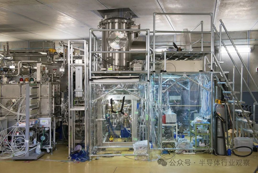
The electron gun injects charge into the compact energy recovery linear accelerator of KEK
In 2021, before severe inflation affected the global economy, the KEK team estimated that the construction cost of a new system (excluding land) was 40 billion yen (260 million US dollars), which could provide 10 kilowatts of EUV and power multiple lithography machines. The estimated annual operating cost is approximately 4 billion yen. Therefore, even considering recent inflation, "the estimated cost of each exposure tool in our device is still quite low compared to the estimated cost of plasma sources generated by lasers today," Nakamura said.
Nakamura acknowledges that there are still many technical challenges that need to be addressed before such a system can achieve the high performance and operational stability required by semiconductor manufacturers. The team must develop new versions of key components such as superconducting cavities, electron guns, and oscillators. Engineers must also develop good programming techniques to ensure that the electron beam does not decay or fail during operation.
To ensure that their method is cost-effective enough to attract the attention of chip manufacturers, researchers need to create a system that can reliably transmit over 1 kW of EUV power to multiple lithography machines simultaneously. Researchers have designed a special arrangement concept for mirrors that can transmit EUV light to multiple exposure tools without causing power loss or damage to the mirrors.
Other EUV possibilities
For rapidly expanding chip manufacturers, the development of EUV free electron lasers is still too early and not worth paying attention to. But the KEK team is not the only team pursuing this technology. XLight, a venture capital backed startup located in Palo Alto, California, is also among the teams pursuing this technology. The company has gathered senior particle accelerator professionals from institutions such as Stanford Linear Accelerator, and recently signed a research and development agreement with Fermi National Accelerator Laboratory in Illinois to develop superconducting cavity and low-temperature module technology.
According to xLight, the mission of the company's establishment is to create a light source that can completely change lithography, metrology, and testing. They stated that the reason for this goal stems from the belief that the United States must regain and maintain its leadership position in semiconductor manufacturing.
XLight has developed an extremely ultraviolet (EUV) light source for cutting-edge semiconductor device manufacturing, which has significant competitive advantages in performance, productivity, and sustainability. The xLight light source is based on mature particle accelerator technology, and system engineering focuses on mass production requirements. Therefore, this new light source reliably provides functionality and adjustability that can change the current manufacturing process, while also achieving the lithography, metrology, and detection functions required for the next generation architecture and process nodes.
XLight generates a new EUV light source that will give the United States a leading position in the future semiconductor industry.
The reporter attempted to contact xLight, but did not receive a response. However, in January, the company participated in the 8th EUV-FEL seminar held in Tokyo, where former CEO Erik Hosler gave a speech on the technology.
It is worth noting that ASML considered turning to particle accelerators a decade ago, and recently when comparing the progress of free electron laser technology with laser plasma roadmaps, ASML also considered turning to particle accelerators. But company executives believe that the risk of LLP is relatively small.
In fact, this is a path full of risks. Independent opinions on the KEK project emphasize that reliability and funding will be the biggest challenges for researchers in the future. "The R&D roadmap will involve many demanding stages to develop a reliable and mature system," Hassanein said. "This will require significant investment and a considerable amount of time."
"Machine design must be extremely robust and have built-in redundancy," retired research scientist Benson added. The design must also ensure that components are not damaged by radiation or laser And this must be achieved "without affecting performance, and the performance must be good enough to ensure good energy conversion efficiency."
More importantly, Benson warned that without a commitment to immediately invest in the technology, "the development of EUV-FEL may not arrive in a timely manner to help the semiconductor industry."
By the way, do you all seem familiar with this plan? Because two years ago, domestic self media had already circulated a related plan. But at that time, you can refer to the report for comments.
*Disclaimer: This article is original by the author. The content of the article is the author's personal opinion. Reproduction on Huanian Mall is only for the purpose of conveying a different viewpoint, and does not imply that Huanian Mall agrees or supports this viewpoint. If you have any objections, please feel free to contact Huanian Mall.


