Abstract: This article provides an overview of the thermal characteristics and design of IGBT modules, introduces the thermal impedance network model of IGBT modules, and its relationship with the thermal performance and size of packaging materials; Discuss the key points of thermal design for modules from the aspects of chip and module packaging materials, structure, etc., and explain the thermal design of traditional IGBT modules and new crimping IGBT modules.
Keywords: semiconductor; IGBT module; Thermal design; Reliability; Cooling solution
introduction
High power semiconductor devices are the units that achieve energy generation, transmission, conversion, and control, and are the most core components of power electronic systems. They largely determine the performance, efficiency, reliability, cost, volume, and weight of power systems. At present, in the field of high-power semiconductor devices with a voltage of 600 V and above, the mainstream products are silicon-based insulated gate bipolar transistors (IGBTs) and corresponding freewheeling diodes (FWDs). The basic unit of power semiconductor devices is the chip, and due to factors such as yield, consistency, and manufacturability, the size of IGBT chips is generally less than 200 mm2, with a maximum current of around 300 A. In order to meet the requirements of high-power systems, IGBT and FWD chips are generally packaged in parallel as IGBT module structures. In addition to achieving electrical interconnection between chips, connecting dynamic units and external main circuits, IGBT modules also play a supporting, protective, and heat dissipation role.
As an application unit of high-power semiconductor devices, the packaging form, structure, technology, and materials of IGBT modules largely determine the overall performance and reliability of the modules. Therefore, the packaging technology of IGBT modules is of crucial significance to the industry and users. The design, manufacturing, testing, and reliability of IGBT modules have always been one of the key topics in power semiconductor research and development.
This article mainly outlines the thermal behavior and design of traditional IGBT modules, as well as the thermal design method of new pressure bonded IGBT modules. Discuss the relationship between thermal resistance and the thermal performance and size of packaging materials through the thermal impedance network model of IGBT modules. Discuss the impact of power loss in power semiconductor devices on junction temperature and temperature changes on module lifespan. And analyze the key points of module thermal design from the aspects of chip and module packaging structure, materials, etc., as well as the thermal management scheme of IGBT modules in application systems.
1. Thermal Resistance Network of IGBT Module
The structural cross-sectional diagram of the traditional IGBT module is shown in Figure 1. The chip is insulated from the outside through a ceramic lining plate, and the substrate plays a role in heat dissipation, support, and contact with the external heat sink. Electrical interconnection and connection are achieved through aluminum wire bonding and solder layer.
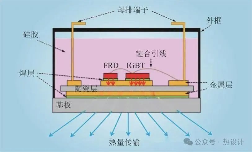
Figure 1 Cross section diagram of traditional IGBT module structure
The aluminum bonding lead of the module has a smaller bonding point with the chip, and the heat generated during chip operation is mainly transmitted unidirectionally from the chip to the substrate through thermal conduction. During this process, certain resistance will be encountered, which is called thermal resistance. The thermal resistance Rth j-c from the chip to the shell is the sum of the series connected thermal resistances of each layer of material on the heat dissipation path. According to equation (1), the thermal resistance and heat capacity of each layer of material are determined by its heat dissipation area and thickness, and the heat dissipation area is determined by the material's thermal diffusion angle α.

In the formula: Rth is the thermal conductivity and resistance of the material; D is the thickness of the thermal conductive medium layer; K is the thermal conductivity; A is the area of the thermal conductive medium; C is the heat capacity; C is the specific heat capacity of the material; M is the material quality. On the heat dissipation path of the IGBT module, from the chip downwards, the heat dissipation area A gradually increases. Assuming that the heat dissipation angle α is constant and the heat conduction area is square, as shown in Figure 2, the area of the i-th layer of heat conduction medium Ai is approximately estimated by equation (2).

In the formula: di represents the thickness of the i-th layer of medium; Li − 1 is the side length of the i-1 layer thermal conductive medium.

Figure 2: Heat dissipation area of different media on the heat dissipation path of IGBT module
According to the Cauer model, the equivalent thermal resistance network of traditional IGBT modules is shown in Figure 3. This model is based on practical physical meaning, equating the overall thermal resistance to the sum of the thermal resistances of each layer of thermal conductive medium, and the heat capacity of each medium is determined by its material properties and quality. According to this model, the Rth j-c of the IGBT module can be calculated.

Figure 3 Cauer model of equivalent thermal resistance network for IGBT module
Thermal design and management of 2 IGBT modules
The Rth j-c of IGBT modules is directly related to the chip area. The larger the chip area, the larger the cross-sectional area of the heat dissipation channel, and the smaller the Rth j-c. However, in order to improve the power density of modules and power systems, reduce the volume, the current research and development focus is gradually increasing the current density of the chip, reducing the overall area of the chip, and thus increasing the Rth j-c. By using the wafer process, chip power consumption and Rth j-c can be reduced to a certain extent. In the design of IGBT modules, it is necessary to optimize the structure and materials to reduce the increase in thermal resistance caused by high power density chips. And by increasing the Tjmax of the chip, the margin of thermal design and the reliability of the module are increased.
2.1 The influence of packaging materials on thermal characteristics
In addition to semiconductor chips, the packaging materials for traditional IGBT modules mainly include insulation lining boards, busbar terminals, bonding leads, solder, substrates, silicone, plastic shells, etc. The key to material thermal design is to choose a combination of materials with high thermal conductivity and CTE matching rate, in order to reduce thermal resistance and thermal mechanical stress. Thermal mechanical stress is the main cause of thermal fatigue degradation and failure of power modules, which is caused by different CTE of materials during temperature changes, and has the greatest impact on the bonding layer and interconnection part of the modules. Therefore, optimizing the selection of module materials based on thermal characteristics is an important step in improving the thermal stability and lifespan of modules.
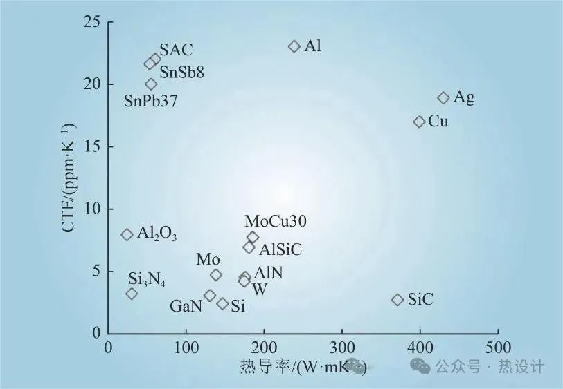
Figure 4 Thermal characteristics of commonly used packaging materials for IGBT modules
Figure 4 shows the main thermal parameters of commonly used packaging materials for IGBT modules. At present, the commonly used insulation lining boards mainly include Al2O3, AlN, Si3N4, etc. In terms of thermal characteristics, AlN is a relatively ideal packaging material and the primary choice for most IGBT modules. However, Al2O3 has cost advantages, while Si3N4 has mechanical strength advantages, and specific considerations need to be made in design according to application requirements. The commonly used chip interconnect material for IGBT modules is Al bonded leads, but their thermal and electrical conductivity are weaker than Cu materials, and their CTE is larger than Cu. Under temperature shock, they are subjected to greater thermal mechanical stress and lower reliability. Therefore, copper wire bonding has advantages in electrical, thermal, and reliability, and is a development trend in power module packaging materials and technology.
At present, the substrate materials for IGBT modules mainly include Cu, AlSiC, and Cu alloy. Cu materials have high thermal conductivity, but CTE differs significantly from materials such as Si and lining plates, which can easily generate large thermal mechanical stresses during operation. AlSiC has a higher CTE matching degree with other materials in the module system, and a relatively high thermal conductivity, making it a commonly selected packaging material for high reliability modules.
For sealing materials such as silicone and casing, the working temperature range and thermal stability are key parameters that need to be considered. They are generally tested through high and low temperature storage and impact tests, especially for power modules applied under harsh temperature conditions. Temperature characteristics and stability are important assessment indicators for module sealing materials.
2.2 Thermal design scheme for module structure
The structure of IGBT modules to some extent determines their thermal resistance. Figure 3 is an equivalent thermal resistance network based on the traditional IGBT module structure, which characterizes Rth j-c as determined by the heat dissipation path of the module structure. In applications, the heat transmitted to the module casing will be carried away by the external heat sink, so the thermal resistance Rth c-h from the module to the heat sink is an important part of module thermal design and management. The thermal resistance Rth j-h from the chip to the external heat sink can be expressed as

In application, a thermal conductive silicone grease with a thickness of about 0.1 mm is generally applied between the flat substrate shell of traditional modules and the heat sink to fill the gap when the substrate contacts the heat sink, increasing heat dissipation efficiency. Due to the low thermal conductivity of thermal conductive silicone grease, Rth c-h generally accounts for about 50% of the overall thermal resistance Rth j-h. Through module packaging structure design, such as direct heat dissipation, the thermal conductive silicone grease layer can be removed in applications, significantly reducing the overall thermal resistance.
2.2.1 Direct water-cooled heat dissipation structure
Figure 5 is a schematic diagram of the structure of a direct liquid cooled (DLC) IGBT module. Using a pin fin structure substrate, direct liquid cooling is achieved without the need for a thermal conductive silicone grease layer and an external heat sink in applications. Compared with traditional flat substrate structures, the Rth j-h is reduced by about half, as shown in Figure 6.
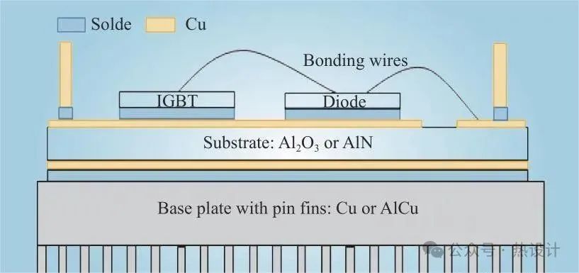
Figure 5 DLC IGBT module structure
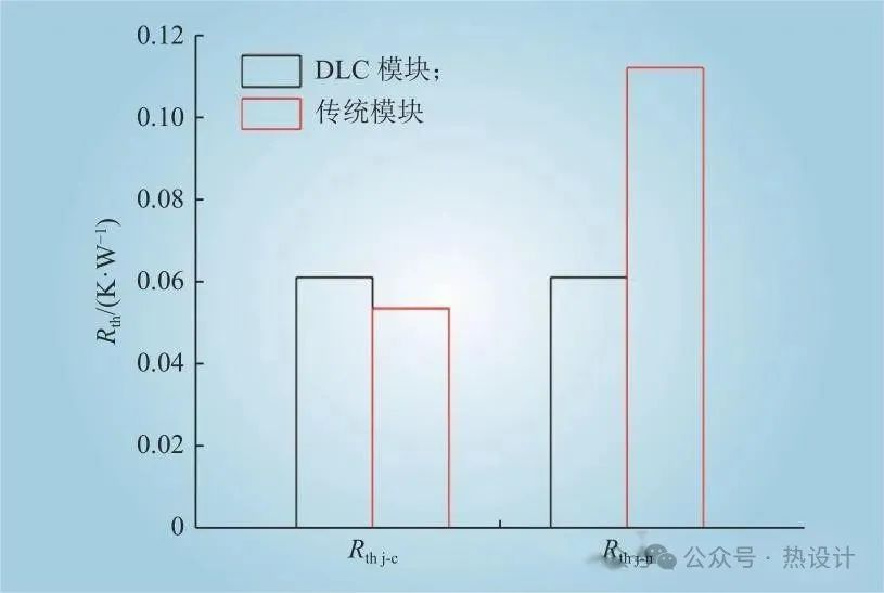
Figure 6 Comparison of thermal resistance between DLC and traditional structured IGBT modules
2.2.2 Double sided heat dissipation structure for flat packaging
The planar packaging structure uses a metal layer to replace the aluminum bonded lead interconnect on the chip surface, which can reduce electrical parasitic parameters, improve current carrying capacity, and has a series of advantages in electrical, thermal, mechanical, and reliability aspects.
Through the flat packaging structure and technology, the heat loss generated by IGBT modules can be diffused through heat sinks in both the upper and lower directions, achieving the effect of double side cooling (DSC). The calculation formula for the equivalent thermal resistance of the Rth j-c DSC structure is shown in equation (4), where Rth j-c T and Rth j-c B are the thermal resistances of the chip to the upper and lower surfaces of the shell, respectively. By adopting a symmetrical design, the heat dissipation efficiency of the module can be doubled, and the equivalent Rth j-c can be reduced by about half, greatly reducing Tj and improving thermal performance and temperature reliability.

Figure 7 is a schematic diagram of the structure of the latest DSC flat package automotive IGBT module developed by CRRC Era Electric in Zhuzhou. The power chip is connected to two layers of insulation lining plates through welding or silver sintering technology, and the current channel passes through the copper coating layer of the upper lining plate. The heat generated by the chip diffuses through two layers of lining plates to the external heat sink. The module casing is formed through mold transfer technology, which has high operating temperature and reliability.
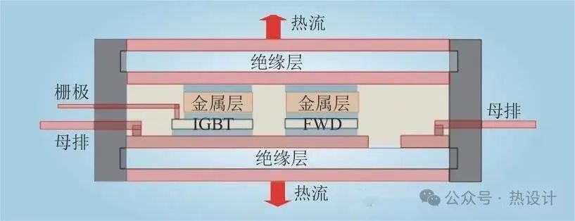
Figure 7 Structure of DSC IGBT module in planar packaging
The DSC module does not have a substrate, and its Rth j-h is more than 50% lower than that of the DLC module. However, due to the lack of integrated direct water-cooled radiators, applications require contact with external radiators through thermal conductive materials or welding, thereby increasing the Rth j-h. Figure 8 shows the equivalent Rth j-h of the DSC module under different installation methods and its comparison with the DLC module. The Rth j-h of DSC modules installed by crimping thermal conductive materials is reduced by about 30% compared to DLC modules, which is influenced by the thermal conductivity of the thermal conductive materials; The Rth j-h of the DSC module installed by welding is reduced by about 40% compared to the DLC structure.

Figure 8 DSC module Rth j-h and its comparison with DLC module
2.2.3 Integrated phase change structure heat dissipation structure
Phase change heat dissipation involves changing the material state of phase change materials to absorb heat, such as the process of liquid evaporation into gas. A heat pipe or steam chamber is a structure that utilizes liquid phase change processes to achieve heat dissipation, with high heat dissipation efficiency. It has been applied in the thermal management of power semiconductor devices and systems. But this structure is generally designed for external heat dissipation and applied outside the power module. When the heat pipe or steam chamber structure is integrated into the module package, efficient heat dissipation and compact packaging will be achieved.
Figure 9 shows a cross-sectional view of an IGBT module with a substrate integrated phase change cooling (PCC) structure. The simulation results show that compared with traditional structures, the integrated phase change structure can reduce thermal resistance by about 15%. CRRC Times Electric has developed an electric vehicle level power module based on this design, as shown in Figure 10.
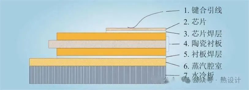
Figure 9 IGBT module with integrated phase change heat dissipation structure on substrate
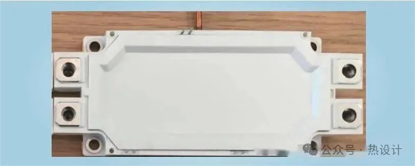
Figure 10 Integrated phase change heat dissipation structure IGBT module sample
The thermal design of other module structures also includes substrate free structures, liner free structures such as direct chip bonding to the die on lead frame (DOL), liner direct liquid cooling, integrated design of liner substrate, and integrated liquid circulation cooling channels. The design goal is to simplify the module structure, reduce the number of bonding layers, remove thermal interface materials (TIM), achieve a reduction in thermal impedance, lower Tj, and increase thermal stability and reliability.
In terms of module packaging technology, advanced combination and interconnection technology can significantly improve the thermal stability of modules. Developing welding, sintering, and lead wire materials with higher thermal conductivity, or using large-area metal sheets instead of lead wire bonding techniques, such as direct lead bonding (DLB), can increase flow and thermal conductivity, achieve uniform temperature distribution, and reduce overheating. Using ultrasonic bonding technology for terminal connection, removing the bonding layer between the terminal and the backing plate can significantly reduce thermal mechanical stress and improve thermal stability.
2.3 Comparison of thermal resistance of different packaging structures
The junction coolant thermal resistance (Rth j-f) was tested for IGBT modules with different heat dissipation structures, as shown in Figure 11. Among the above three structures, the DSC module has the highest heat dissipation efficiency and the lowest thermal resistance, making it the development trend of the next generation of high-power density IGBT modules. The experimental results have verified that the heat dissipation efficiency of PCC structure is about 15% higher than that of DLC structure, and it has good application prospects to a certain extent and within a certain range. However, in the coming period, due to the advantages of manufacturing process and simple application, DLC modules will still be the mainstream product in high-performance and high reliability IGBT modules such as electric vehicles.
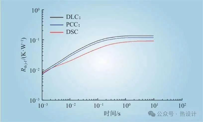
Figure 11 Comparison of thermal resistance of IGBT modules with different heat dissipation structures
2.4 Thermal design of crimped IGBT modules
The press pack IGBT (PPI) module is an ideal switching device for ultra-high voltage flexible DC transmission systems, and its fully controllable turnoff capability is the most critical requirement for voltage source converters in the system. The current newly-built ultra-high voltage direct current transmission projects have entered the stage of replacing high-power thyristors with IGBT modules. For example, the Zhangbei and Wudongde projects, which have recently completed system tests, have partially and completely adopted PPI modules, achieving the world's highest voltage level and largest transmission capacity for flexible direct current transmission.
The packaging concept and structure of PPI modules come from high-power thyristors. Large area power terminals are connected to the front and back of multiple chips through pressure, forming parallel connections and improving power capabilities. Through design, the crimping packaging structure can achieve the goals of double-sided heat dissipation, failure short circuit, etc. This is a key requirement for systems such as high-voltage direct current transmission systems that require multiple power devices to be connected in series to achieve high voltage. However, the non planar interconnect structure of traditional welded IGBT modules is inferior to PPI modules in terms of power capacity, heat dissipation, short circuit failure, reliability, and other aspects.
Figure 12 shows the basic structural units and module structure sectional view of CRRC Era's electrical PPI module products. Its basic units are composed of chips, metal spacers, gate connection pins, and insulation frames. Through module level packaging, multiple basic units are packaged in parallel within the module. Its main components include ceramic shells, covers, sockets, gate circuit PCBs, etc. Therefore, the thermal design of PPI modules includes two aspects: basic unit level and module level.
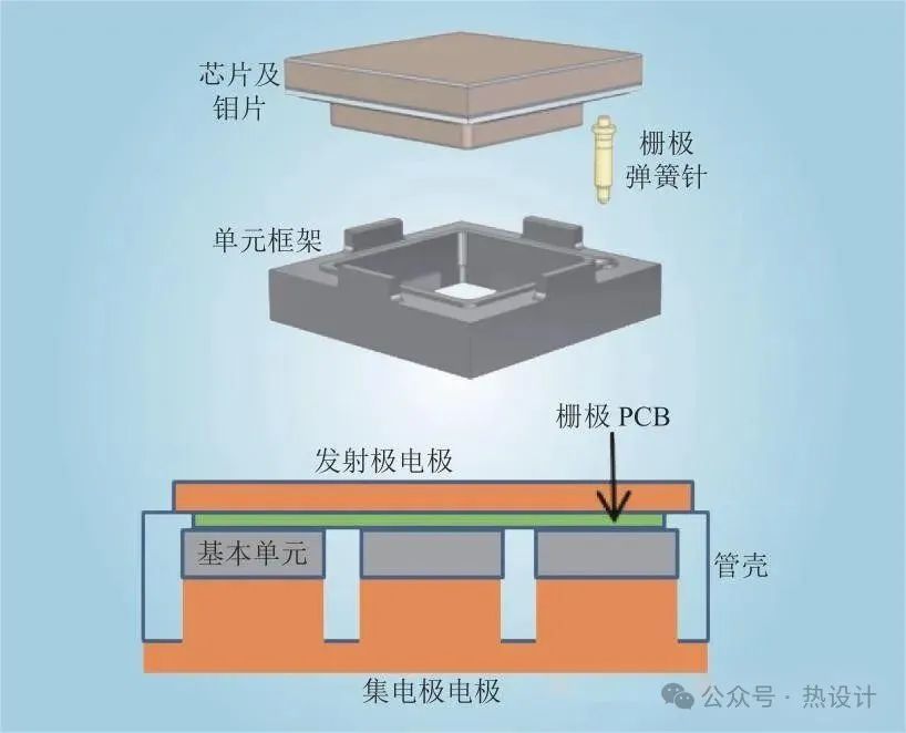
Figure 12 Basic structural units and overall structural sectional view of PPI module
Based on the materials, dimensions, processes, and application conditions used in the PPI module, an accurate thermal simulation model can be established. This information can be characterized in a reasonable way in the thermal model, and the temperature field distribution shown in Figure 13 can be output for thermal management design and optimization of the PPI module. Figure 14 shows the transient thermal impedance curves of the PPI module under different pressures. As the pressing force increases, the contact thermal resistance of the device decreases, the overall thermal resistance decreases, and the change in thermal resistance also decreases. According to its variation pattern, the range of pressing force can be calibrated.
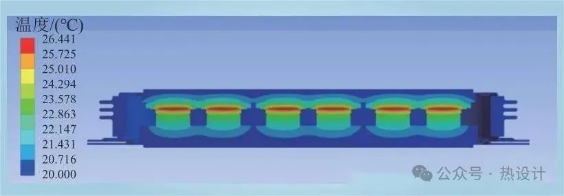
Figure 13 Temperature distribution cloud map of PPI module under application conditions
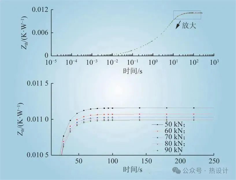
Figure 14 Transient thermal impedance curves of PPI module under different pressures
3 Conclusion
The thermal performance and stability of IGBT modules are important aspects of module design, characterization, and application evaluation. The key to packaging and application design is to achieve fast and efficient cooling of chips, which will greatly improve the performance of IGBT modules, reduce chip junction temperature and power loss, and thus improve stability and reliability. Especially with the increase in power density of IGBT modules, harsh application environments, and higher requirements for reliability and lifespan, the thermal design and management technology of IGBT modules are the most important links in the design and application of new products.
This article mainly outlines the thermal behavior and design technology of traditional IGBT modules, as well as the thermal design of crimped IGBT modules for flexible DC transmission grid applications. Based on the thermal impedance network model of IGBT modules, this paper discusses the thermal design and management scheme of IGBT modules from the aspects of packaging materials, structure, and process technology. By combining new high thermal performance materials, integrated packaging structures, and high temperature stability packaging technology, the thermal performance, reliability, and lifespan of IGBT modules can be enhanced and improved.


