In the past 8 months, Qualcomm has made many interesting statements about its high-performance Windows on Arm SoC, many of which will be tested in the coming weeks. But in the increasingly competitive environment of PC CPUs, besides all performance claims and promotions, there is a more fundamental question about Snapdragon X that we have always been eager to know: how does it work?
Before the release next week, we finally got the answer because today Qualcomm released their long-awaited Snapdragon X SoC architecture disclosure. This includes not only their new custom Arm v8 "Oryon" CPU core, but also their Adreno GPU technology disclosure, as well as the Hexagon NPU that supports their heavily promoted AI functionality.
The company has clearly stated in the past that Snapdragon X is a serious and prioritized plan for the company - they will not just piece together existing IP modules into Windows SoC - so there are many new technologies in SoC.
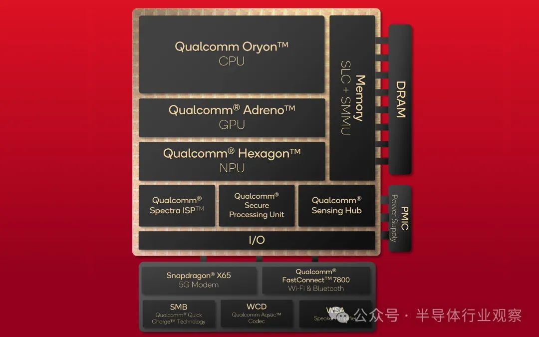
Although we are pleased to see all of this, we must first admit that what excites us the most is finally being able to gain a deeper understanding of Oryon, the ARM CPU core customized by Qualcomm. As the first new high-performance CPU design created from scratch in the past few years, the importance of Oryon cannot be overstated. In addition to providing the foundation for the next-generation Windows on Arm SoC (which Qualcomm hopes to gain a foothold in the Windows PC market), Oryon will also become the foundation for Qualcomm's traditional Snapdragon mobile and tablet SoC.
Therefore, in the coming years, a large amount of the company's hardware will be based on this CPU architecture - if everything goes according to plan, Oryon will launch more generations of products. Anyway, it will make Qualcomm stand out from its competitors in both PC and mobile fields, as it means Qualcomm is breaking away from Arm's reference design, which is essentially Qualcomm's competitor.
Without delay, let's delve deeper into Qualcomm's Snapdragon X SoC architecture.
Elite, Plus, and currently released SKUs
To briefly review, Qualcomm has announced four Snapdragon X SKUs so far, all of which have been made available to device manufacturers and will be launched next week.
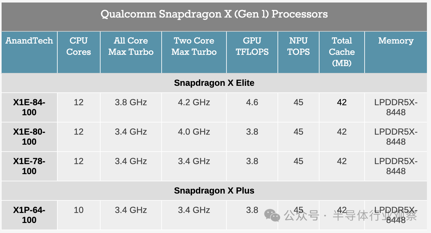
Three of them are "Elite" SKUs, which contain 12 CPU cores. At the same time, Qualcomm has only launched one "Plus" SKU, reducing its CPU core count to 10.
Officially, Qualcomm has not specified any TDP level for these chip SKUs, as in principle, any given SKU can be used throughout the entire power level range. Need to install top-level chips in fanless laptops? Just lower the TDP to match your power/cooling capacity. That is to say, to achieve the maximum clock speed and performance goals of Qualcomm chips, a large amount of cooling and power transmission is required. For this reason, we are unlikely to see X1E-84-100 appear in fanless devices, for example, as its higher clock speed would be wasted due to a lack of cooling space. This will not prevent lower performing chips from being used as budget options for larger devices, but SKU tables can also be seen as roughly sorted by TDP.
Although this is not what was disclosed today, don't be surprised to see more Snapdragon X chip SKUs about to be launched. Qualcomm has at least one Snapdragon X chip under development, which has become a little-known secret - a smaller chip with potentially fewer CPU and GPU cores - and may launch a more budget focused SKU series in the future. But currently, Qualcomm is starting with its large chips, making it its highest performing choice.
Although the first batch of Snapdragon X devices will not be available to consumers until next week, based on OEM adoption, this will clearly be Qualcomm's most successful Windows on Arm SoC to date. Compared to Snapdragon 8cx Gen 3, the difference in adoption is almost a world apart; Qualcomm's PC partners have developed over a dozen laptop models using new chips, and the latest 8cx has two designs. Therefore, as companies such as Microsoft, Dell, HP, and Lenovo are all producing Snapdragon X laptops, the Snapdragon X ecosystem has started much stronger than any previous Windows on Arm product.
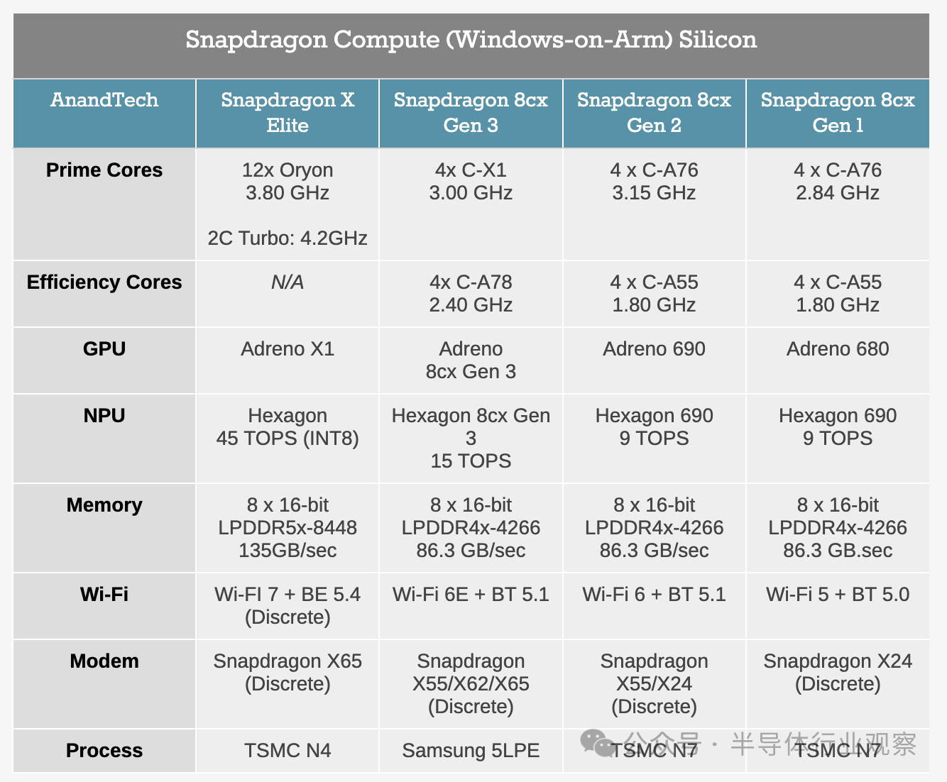
Undoubtedly, this is largely attributed to the powerful architecture of Qualcomm. Snapdragon X is equipped with a CPU that Qualcomm claims to be much more powerful than the Cortex-X1 core on the latest (approximately 2022) 8cx chip, and is manufactured using a highly competitive process with TSMC N4 nodes. Therefore, if all conditions are correct, Snapdragon X chips should be a huge advancement for Qualcomm.
At the same time, there are two other pillars supporting the release of this product. The first one, of course, is artificial intelligence. Snapdragon X is the first Windows SoC to support Copilot+. Snapdragon X's Hexagon NPU requires 40+TOPS NPUs, and the 45 TOPS Hexagon NPU makes this SoC the first chip to provide such high performance for neural networks and other model inference. The second pillar is performance. Qualcomm promises that with years of experience in producing mobile SoCs, the battery life of its SoCs will be very long. If they can achieve this goal while also achieving performance goals - allowing users to have both fish and bear's paw - then it will provide a solid foundation for Snapdragon X chips and the resulting laptops.
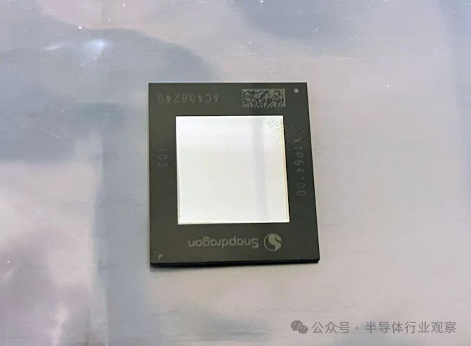
Ultimately, Qualcomm hopes to achieve their Apple Silicon moment - repeating the performance and battery life improvements Apple achieved when transitioning from Intel x86 chips to their own custom Arm chip, Apple Silicon. And its partner Microsoft is very, very eager to have a competitor to MacBook Air in the PC ecosystem. This is a daunting task, and the most important reason for it is that both Intel and AMD have not stagnated in the past few years, but this is not unattainable.
Nevertheless, Qualcomm and the Windows on Arm ecosystem do face some obstacles, which means that the release trajectory of Snapdragon X will never be on par with Apple. In addition to the obvious lack of a unified development hardware and software ecosystem (and driving developers to develop software for it), Windows also comes with expectations for backward compatibility and the resulting legacy burden. Microsoft, on the other hand, continues to focus on its x86/x64 simulation layer, now called Prism, and the release of Snapdragon X will be its first true test. But even though Windows has been supporting Arm for many years, the software ecosystem is still slowly taking shape, so Snapdragon X will rely more on x86 simulation than Apple. Windows and macOS are very different operating systems, and this was particularly evident in the first few years of Snapdragon X, both in terms of their history and the development philosophy of their owners.
Oryon CPU Architecture: A Carefully Designed Core for All Applications
To delve deeper into the architecture, we will start with the most core part: the Oryon CPU core.
To briefly review, Oryon is essentially a third-party acquisition by Qualcomm. The CPU core was originally named "Phoenix" and was developed by chip startup NUVIA. NUVIA itself is composed of several former Apple employees, and its initial plan was to develop a new server CPU core that would compete with the cores in modern Xeon, EPYC, and Arm Neoverse V.
However, Qualcomm seized the opportunity to acquire an excellent CPU development team and acquired NUVIA in 2021. Phoenix has been repurposed for consumer grade hardware and reborn as the Oryon CPU core.
Although Qualcomm did not pay much attention to the root cause of Oryon, it is clear that the first generation architecture (using Arm's v8.7-A ISA) is still deeply rooted in the original Phoenix design. Phoenix itself has been designed to be scalable and energy-efficient, so this is not a bad thing for Qualcomm. But this does mean that many customer-centric core design changes did not appear in the initial Oryon design, and we should look forward to seeing these changes in future generations of CPU architectures.
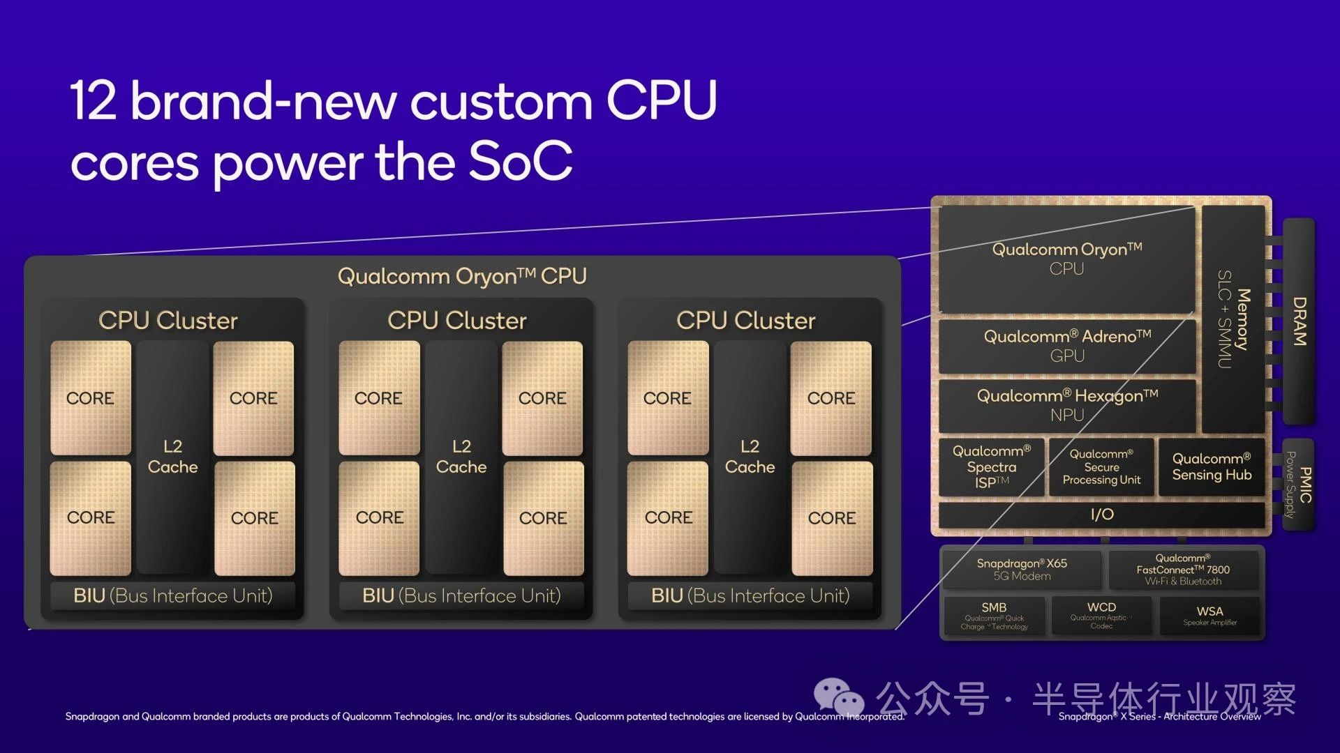
After in-depth research, as previously disclosed by Qualcomm, Snapdragon X uses three sets of Oryon CPU cores. From a high-level perspective, Oryon is designed as a full-size CPU core that can provide both energy efficiency and performance. For this reason, it is the only CPU core required by Qualcomm; It does not have a separate core for performance and efficiency optimization like Qualcomm's previous Snapdragon 8cx chips or Intel/AMD's latest mobile chips.
According to Qualcomm, all clusters are equal. Therefore, no "efficiency" cluster is adjusted for power efficiency rather than clock speed. However, only 2 CPU cores (in different clusters) can achieve the maximum turbocharging speed of any given SKU; The maximum speed of the remaining cores reaches the full core turbocharging speed of the chip.
And each cluster has its own PLL, so each cluster can be timed and powered on separately. In fact, this means that when the workload is low, both clusters can enter sleep mode and then wake up from sleep mode when more performance is needed.

Unlike most CPU designs, Qualcomm has adopted a flatter cache hierarchy for Snapdragon X and Oryon CPU core clusters. L2 cache is not shared by every core, but by every four cores (which is very similar to how Intel shares L2 cache on its E core cluster). Moreover, this is also a fairly large L2 cache, with a size of 12MB. L2 cache is associated with 12 channels, and even if it is so large, the delay in accessing L2 cache after L1 miss is only 17 cycles.
This is an inclusive cache design, therefore it also includes mirroring of the content in L1 cache. According to Gao Tong, they use inclusive caching for energy-saving reasons; Inclusive caching means eviction is much simpler because L1 data does not need to be moved to L2 to be evicted (or deleted from L2 when promoted to L1). Conversely, cache consistency is maintained using the MOESI protocol.
The L2 cache itself runs at full core frequency. The L1/L2 cache operation is a full 64 byte operation, which is equivalent to hundreds of GB of bandwidth per second between the cache and the CPU core. Although L2 caching is mainly used to serve its own directly connected CPU cores, Qualcomm has also implemented optimized cluster to cluster listening operations to cope with situations where one cluster needs to read from another cluster.
Interestingly, the 4-core cluster configuration of Snapdragon X is not even as large as the Oryon CPU cluster. According to Qualcomm engineers, the cluster design actually has all the functions and bandwidth required to handle 8-core designs, which undoubtedly recalls its roots as a server processor. For consumer grade processors, multiple smaller clusters provide higher granularity for power management and can serve as better basic building blocks for manufacturing low-end chips (such as Snapdragon Mobile SoC), but when these cores are located in different clusters (and therefore must be connected to another core through a mainline interface unit), this will bring some trade-offs, namely slower communication speed from core to core. This is a small but noteworthy difference, as the current designs of Intel and AMD both place 6 to 8 CPU cores in the same cluster/CXX/ring.
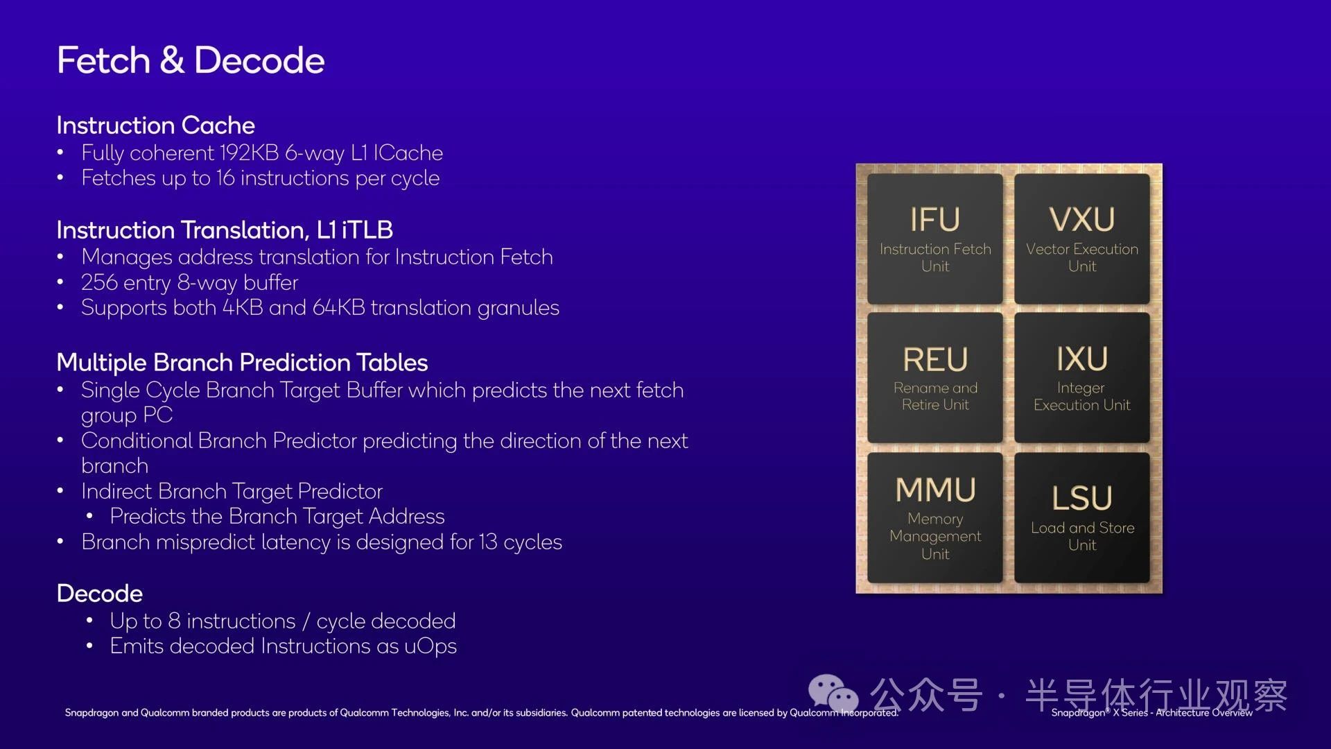
By delving into a single Oryon CPU kernel, we quickly understood why Qualcomm adopts shared L2 cache: the L1 instruction cache in a single kernel is already very large. The Oryon is equipped with a 192KB L1 I-Cache, which is three times larger than the Redwood Cove (Meteor Lake) L1 I-Cache and even larger than the Zen 4. Overall, 6-way associative caching allows Oryon to store a large number of instructions locally in the CPU execution unit. Unfortunately, we do not have L1I latency at hand and cannot compare it with other chips.
In summary, Oryon's fetch/L1 unit can retrieve up to 16 instructions per cycle.
This in turn provides support for a very wide decoding front-end. Oryon can decode up to 8 instructions in one clock cycle, and the decoding front-end is wider than Redwood Cove (6) and Zen 4 (4). And all decoders are the same (symmetrical), so full throughput can be achieved without special circumstances/scenarios.
Like other contemporary processors, these decoded instructions are issued in the form of micro operations (uOps) for further processing by the CPU core. Technically speaking, each Arm instruction can decode up to 7 uOps, but according to Gao, the ratio of Arm v8 instructions to decoded micro operations is usually closer to 1:1.
Branch prediction is another major driving factor for CPU core performance, which is also another area that Oryon is generous with. Oryon has all common predictors: direct, conditional, and indirect. The direct predictor is single cycle; Meanwhile, branch prediction errors can result in a delay loss of 13 cycles. Unfortunately, Qualcomm did not disclose the size of the branch target buffer itself, so we do not know how large they are.
However, we do know the size of the L1 Translation Backup Buffer (TLB), which is used for virtual to physical memory address mapping. This buffer can accommodate 256 entries and supports 4K and 64KB pages.
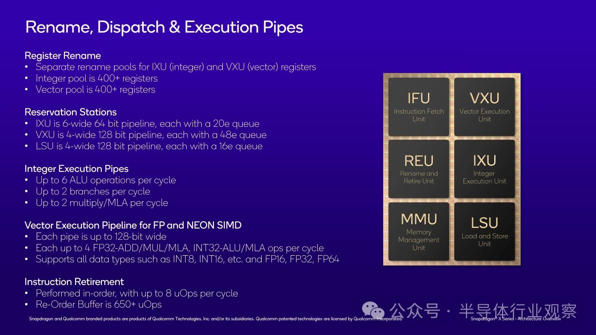
Turning to the execution backend of Oryon, there are many areas worth discussing. Part of the reason is that there is a lot of hardware and a lot of buffers here. Oryon has a considerable 650+reorder buffer (ROB) for extracting instruction parallelism and overall performance through unordered execution. This has made Qualcomm the latest CPU designer, abandoning traditional wisdom and launching a large ROB, avoiding the diminishing returns claimed by larger ROBs.
Conversely, the instruction exit matches the maximum capacity of the decoder block: 8 instruction inputs and 8 uOps outputs. As mentioned earlier, the decoder can technically issue multiple uOps for a single instruction, but in most cases it will perfectly match the instruction exit rate.
The register renaming pool on Oryon is also quite large (do you feel that there is a common theme here?). There are over 400 registers available for integers in total, and an additional 400 registers available for feeding vector units.
As for the actual execution pipeline itself, Oryon provides 6 integer pipelines, 4 FP/vector pipelines, and an additional 4 load/store pipelines. Qualcomm did not provide a complete mapping for each pipeline, so we cannot introduce all possibilities and special circumstances. But at a higher level, all integer pipelines can perform basic ALU operations, while 2 can handle branches and 2 can perform complex multiply accumulate (MLA) instructions. Meanwhile, we are informed that the vast majority of integer operations have a single cycle delay - meaning they are executed within a single cycle.
In terms of floating-point/vector, each vector pipeline has its own NEON unit. Just a reminder, this is an Arm v8.7 architecture, so there are no vector SVE or Matrix SME pipelines here; The only SIMD function of the CPU core is to use the classic 128 bit NEON instruction. This does indeed limit the CPU to narrower vectors than contemporary PC CPUs (AVX2 is 256 bit wide), but it does compensate for this problem through NEON units on all four FP pipes. Moreover, as we are currently in the AI era, FP/vector units support all common data types all the way up to INT8. The only noteworthy omission here is BF16, which is a common data type for AI workloads; But for serious AI workloads, this is the purpose of NPUs.
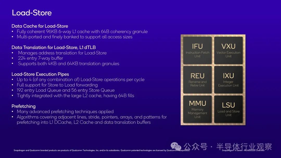
We also saw data loading/storage units on Oryon. The core loading/storage unit is very flexible, which means that the four execution pipelines can perform any combination of loading and storage in each cycle as needed. The loading queue itself can have a maximum of 192 entries, while the storage queue can have a maximum of 26 entries. All padding is the full size of the cache line: 64 bytes.
The L1 data cache itself, which supports loading/storage units, is also quite large. The fully consistent 6-way associated cache size is 96KB, which is twice the size of Intel Redwood Cove cache (although the upcoming Lion Cove will greatly change this). And it has been carefully designed to effectively support various access sizes.
In addition, Qualcomm's memory prefetcher is somewhat like a "secret recipe" because the company states that this relatively complex unit contributes significantly to performance. Therefore, Qualcomm has not disclosed much about the working principle of its prefetcher, but it is undeniable that its ability to accurately predict and prefetch data will have a huge impact on the overall performance of the CPU core, especially at modern processor clock speeds where DRAM has a long travel time. Overall, Qualcomm's prefetching algorithms strive to cover a variety of scenarios, from simple adjacency and span to more complex patterns, using past access history to predict future data demands.
On the contrary, Oryon's memory management unit is relatively simple. This is a fully functional modern MMU that supports more sophisticated features, such as nested virtualization - allowing client virtual machines to host their own client virtual machine management programs to provide services for further virtual machines.
Among the other noteworthy features here, the hardware table traverser is another feature worth mentioning. If the cache row is not in L1 or L2 cache, the unit is responsible for moving the cache row to DRAM, supporting a maximum of 16 times and publishing traversals. Please remember that this is for each core, so a complete Snapdragon X chip can perform a maximum of 192 table traversals at once.
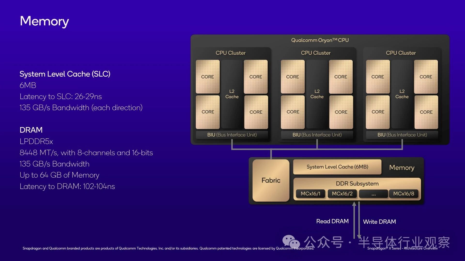
Finally, in addition to the CPU kernel and CPU cluster, we also have the highest level of SoC: the shared memory subsystem.
The last level of cache is located here, sharing L3 cache with the chip. Considering the size of the L1 and L2 cache of the chip, you may think that the L3 cache is also quite large. But you are wrong. In fact, Qualcomm only provides 6MB of L3 cache for its chips, which is only a small fraction of the 36MB L2 cache it supports.
Due to the fact that the chip already has a large amount of cache at the L1/L2 level and these caches are tightly integrated, Qualcomm uses a relatively small sacrificial cache as the last stop before entering system memory. Compared to traditional x86 CPUs, this is a significant change, although it aligns well with Qualcomm's brand positioning, as its Arm Mobile SoC typically has relatively small L3 cache. At least the benefit is that L3 cache access speed is quite fast, with a latency of only 26-29 nanoseconds. And it has the same bandwidth as DRAM (135GB/s), which can transfer data between the L2 cache below it and the DRAM above it.
As for memory support, as previously disclosed, Snapdragon X has a 128 bit memory bus, supports LPDDR5X-8448, and a maximum memory bandwidth of 135GB/s. At the current LPDDR5X capacity, Snapdragon X can handle up to 64GB of RAM. However, I wouldn't be surprised if Qualcomm confirms its support for 128GB after higher density LPDDR5X chips start shipping.
It is worth noting that unlike some other chips focused on the mobile field, Snapdragon X does not use any type of encapsulated memory. Therefore, the LPDDR5X chip will be installed on the device motherboard, and the device supplier can choose their own memory configuration.
Using LPDDR5X-8448 memory, Qualcomm informed us that the DRAM latency should be slightly higher than 100ns, at 102-104ns.
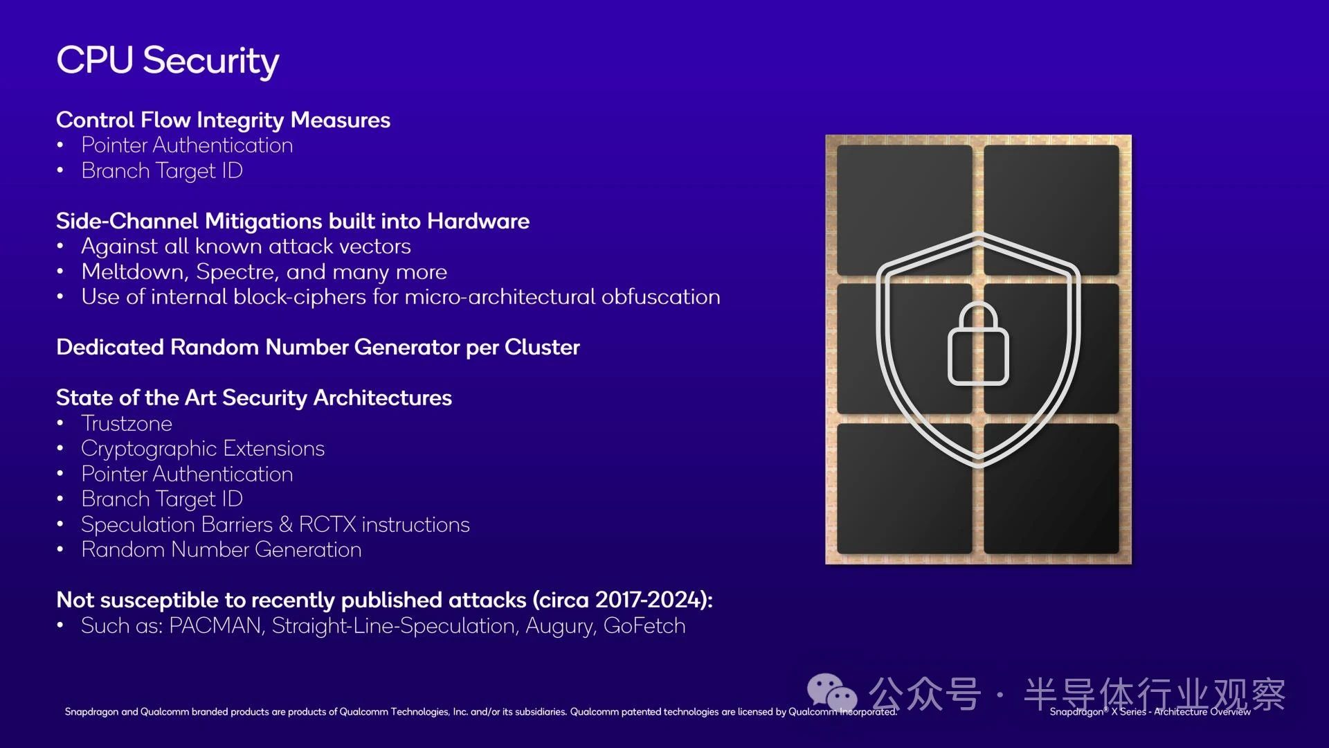
Finally, let's briefly mention CPU security. Qualcomm supports all the security features required for modern chips, including Arm TrustZone, random number generators for each cluster, and security enhancements such as pointer authentication.
It is worth noting that Qualcomm claims that Oryon can alleviate all known bystander attacks, including Spectre, which is known as the "constant gift". This statement is interesting because Spectre itself is not a hardware vulnerability, but rather an inherent consequence of speculative execution. This, in turn, is also the reason why it is difficult to fully defend (the best defense is to isolate sensitive operations on their own). However, Qualcomm believes that by implementing various obfuscation tools in hardware, they can prevent such bypass attacks. So it will be interesting to see how this will develop.
Explanation on x86 simulation
Finally, I would like to take some time to briefly introduce information about x86 simulation on Oryon.
Qualcomm's x86 simulation solution is much more complex than what we are accustomed to on Apple devices, because in the Windows world, no vendor can control both hardware and software stacks simultaneously. Therefore, although Qualcomm can talk about their hardware, they cannot control software issues - and they will not take the risk of collective missteps to speak for Microsoft. Therefore, x86 simulation on Snapdragon X devices is essentially a joint project between two companies, with Qualcomm providing hardware and Microsoft providing the Prism conversion layer.
However, although x86 simulation is largely a software task (Prism takes on most of the heavy workload), Arm CPU vendors can still make certain hardware adjustments to improve x86 performance. And Qualcomm has already made these adjustments. The Oryon CPU core has hardware auxiliary functions that can improve x86 floating-point performance. In order to solve the elephant problem in the room, Oryon also provided hardware adjustments for the unique memory storage architecture of x86- which is widely regarded as one of the key advancements for Apple to achieve high x86 simulation performance on its own chips.
However, no one would think that Qualcomm's chips could run x86 code as quickly as native chips. There will still be some conversion overhead (depending on the workload), and performance critical applications will still benefit from native compilation to AArch64. But Qualcomm is not entirely at the mercy of Microsoft in this regard, as they have made hardware adjustments to improve their x86 simulation performance.
In terms of compatibility, it is expected that the biggest obstacle here is AVX2 support. Compared to the NEON unit on Oryon, the x86 vector instruction set is wider (256b to 128b) and the instructions themselves do not completely overlap. As Qualcomm has stated, the conversion from AVX to NEON is a challenging task. However, we know that this is achievable - Apple quietly added AVX2 support to their game porting toolkit 2 this week - so it will be interesting to see what happens to the next few generations of Oryon CPU cores. Unlike Apple's ecosystem, x86 will not disappear in the Windows ecosystem, so the need to convert AVX2 (ultimately AVX-512 and AVX10!) will never disappear.
Adreno X1 GPU Architecture: A More Familiar Face
Next, let's talk about the GPU architecture of Snapdragon X SoC: Adreno X.
Unlike the Oryon CPU core, Adreno X1 is not a completely new hardware architecture. In fact, three generations of 8cx SoC have already been released before it, and it is not even new to Windows. However, Qualcomm has been secretive about its GPU architecture for many years, so GPU architecture may also be something new for AnandTech readers. It can be said that for over a decade, I have been trying to obtain detailed disclosure information from Qualcomm, and with the launch of Snapdragon X, they have finally achieved this goal.
From a high-level perspective, the Adreno X1 GPU architecture is the latest version of Qualcomm's current Adreno architecture series, with X1 representing the 7th generation. Adreno itself was acquired from ATI 15 years ago (Adreno is a letter inflection of Radeon), and for many years, Qualcomm's Adreno architecture has been the strongest GPU in the Android field.
Of course, the situation in the Windows domain is slightly different because independent GPUs push integrated GPUs aside and cannot handle workloads that absolutely require high GPU performance. Moreover, due to the fact that game development has never completely deviated from GPU architecture/drivers, Qualcomm's insignificant presence in the Windows market for many years has often led to them being overlooked by game developers. However, Qualcomm is not a newcomer to Windows gaming, which gives them an advantage in attempting to gain a larger share of the Windows market.
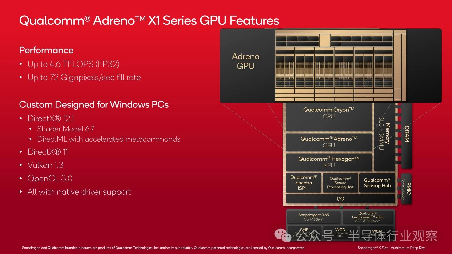
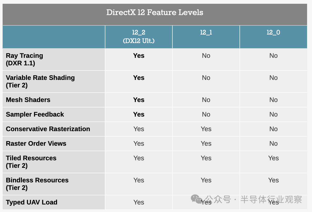
From a functional perspective, the Adreno X1 GPU architecture is unfortunately a bit outdated compared to contemporary x86 SoCs. Although the architecture does support ray tracing, the chip cannot support the complete DirectX 12 Ultimate (functional level 12_2) feature set. This means that it must report itself as a functional level 12_1 GPU to the DirectX application, which means that most games will limit their use of these features.
Nevertheless, Adreno X1 does support some advanced features that have been actively used on Android, as the functionality level of DirectX does not exist. As mentioned earlier, it supports ray tracing, which is publicly available in Windows applications through the Vulkan API and its ray query calls. Considering Vulkan's limited use on Windows, Qualcomm can understand that it will not delve deeper into this topic, but it sounds like Qualcomm's implementation is a level 2 design with hardware ray testing, but without hardware BVH processing similar to AMD's RDNA2.
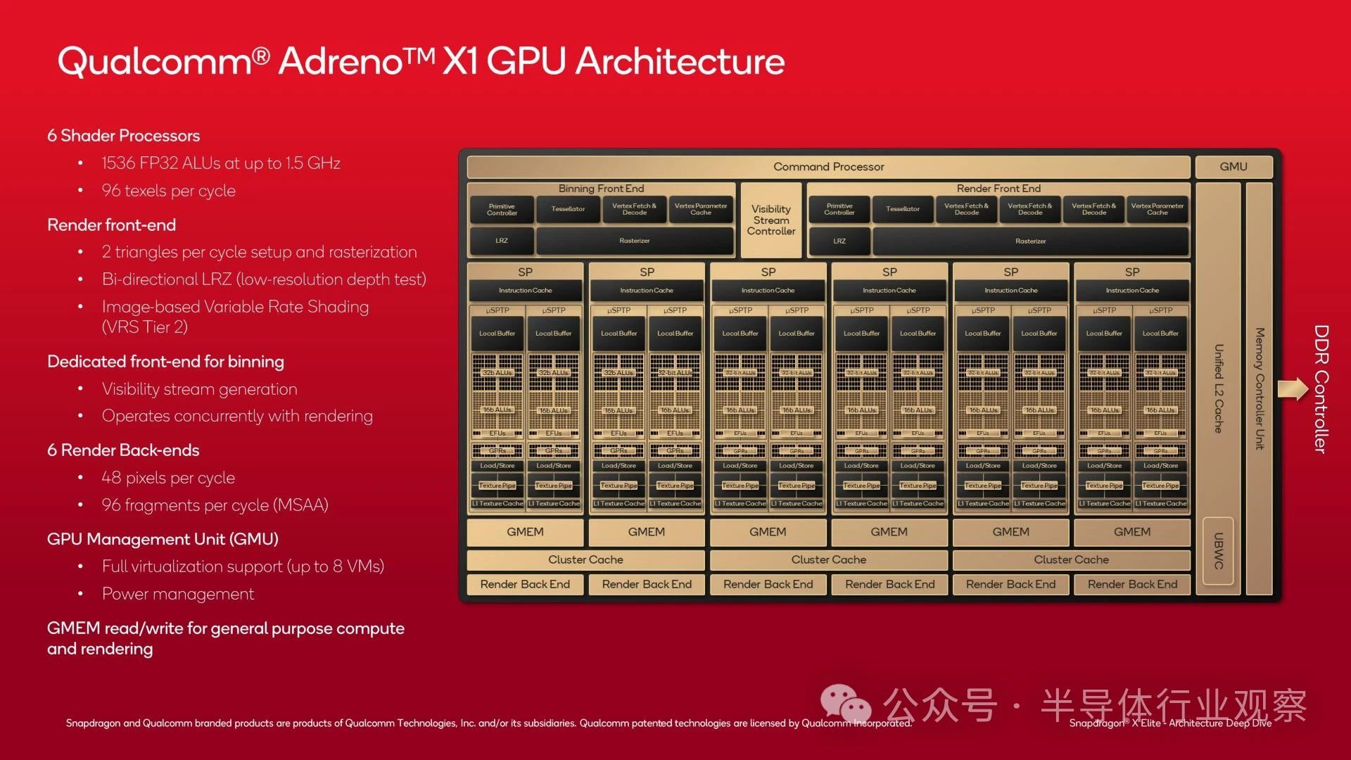
In addition, it also supports Variable Rate Shading (VRS) Layer 2, which is crucial for optimizing shader workloads on mobile GPUs. Therefore, it seems that the feature that hinders X1 from obtaining support for DirectX 12 Ultimate is the feedback from mesh shaders and samplers, which are indeed some significant hardware changes.
In terms of API support, as mentioned earlier, the Adreno X1 GPU supports DirectX and Vulkan. Qualcomm provides native drivers/paths for DirectX 12 and DirectX 11, Vulkan 1.3, and OpenCL 3.0. The only notable exception here is DirectX 9 support, which, like SoC vendor Intel, is implemented using D3D9on12, which converts DX9 commands to DX12. Nowadays, DX9 games are rare (the API was replaced by DX10/11 15 years ago), but since this is Windows, backward compatibility is a continuous expectation.
On the contrary, it even supports Microsoft's new DirectML API for low-level GPU access for machine learning. Qualcomm has even optimized the meta commands written for GPUs so that software utilizing DirectML can run more efficiently without the need to understand any other information about the architecture.
Adreno X1 GPU Architecture Explanation
In addition to advanced features, let's take a look at low-level architecture.
The Adreno X1 GPU is divided into 6 shader processor blocks, each providing 256 FP32 ALUs for a total of 1536 ALUs. The peak clock speed is 1.5GHz, which allows the maximum throughput of the integrated GPU on Snapdragon X to reach 4.6 TFLOPS (lower throughput for low-end SKUs).
Like other GPUs, the front-end of a GPU is divided into traditional front-end/SP/back-end settings, where the front-end is responsible for handling triangle settings and rasterization, as well as merging GPU block based rendering modes. It is worth noting that the GPU front-end can set and rasterize 2 triangles per clock, which will not attract any attention in the PC field in 2024, but is already very good for integrated GPUs. To improve performance, the front-end can also conduct early depth testing to reject polygons that will never be visible before rasterization.
Meanwhile, the backend consists of 6 rendering output units (ROPs), each of which can process 8 pixels per cycle, rendering a total of 48 pixels per clock. Insert the rendering backend into the local cache, as well as the important register memory referred to by Qualcomm as GMEM.
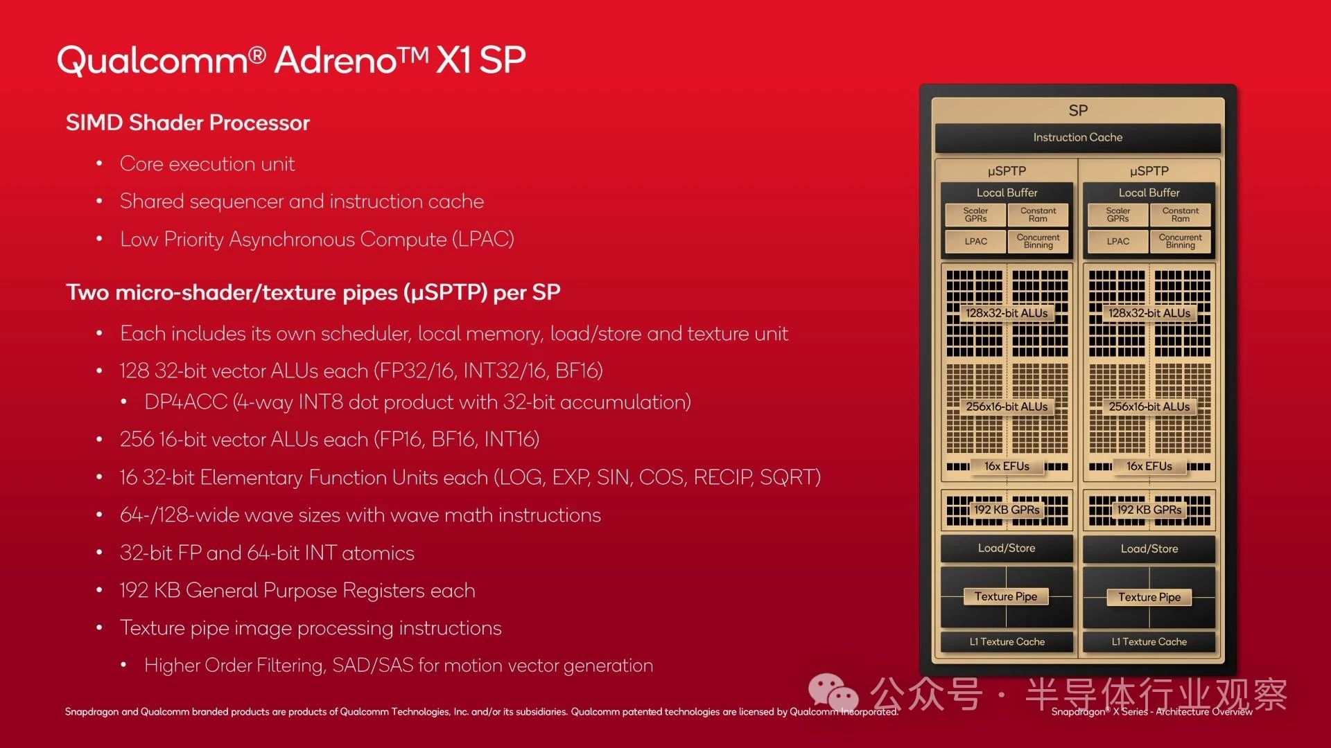
A single shader processor block itself is quite common, especially if you have seen the NVIDIA GPU architecture diagram. Each SP is further subdivided into two microchannels (micro shader pipeline texture pipeline, or uSPTP), controlled by its own dedicated scheduler and other resources (such as local memory, load/store units, and texture units).
Each uSPTP provides 128 FP32 ALUs. Moreover, it is somewhat surprising that there is a separate set of 256 FP16 ALUs, which means that Adreno X1 does not need to share resources when processing FP16 and FP32 data, which is different from the architecture of performing FP16 operations on FP32 ALUs. However, if the GPU scheduler determines the need, the FP32 unit can also be used for FP16 operations.
Finally, there are 16 basic function units (EFUs) used to handle transcendental functions such as LOG, SQRT, and other rare but important mathematical functions.
Surprisingly, the wavefront size used by Adreno X1 is quite large. According to the pattern, Qualcomm uses 64 or 128 channel wide wavefronts. Qualcomm tells us that they typically use 128 wide wavefronts for 16 bit operations (such as fragment shaders), while 64 wide wavefronts are used for 32-bit operations (such as pixel shaders).
In contrast, AMD's RDNA architecture uses a 32/64 wide wavefront, while NVIDIA's wavefront/distortion is always 32 wide. Wide design has fallen out of favor in the PC field because it is difficult to maintain power supply (too much divergence), so this is very interesting. Although people usually worry about wavefront size, considering the high GPU performance of Qualcomm smartphones SoC, it seems to be very effective for Qualcomm - considering the high resolution of phone screens, this is not an easy task.
Except for ALU, each uSPTP contains its own texture unit, and each uSPTP can output 8 texture pixels per clock. There are also limited image processing functions here, including texture filtering, and even SAD/SAS instructions for generating motion vectors.
Finally, there is a considerable amount of register space in each uSPTP. In addition to the L1 texture cache, there are a total of 192KB general-purpose registers used to provide information for each block and attempt to hide delay bubbles in the wavefront.

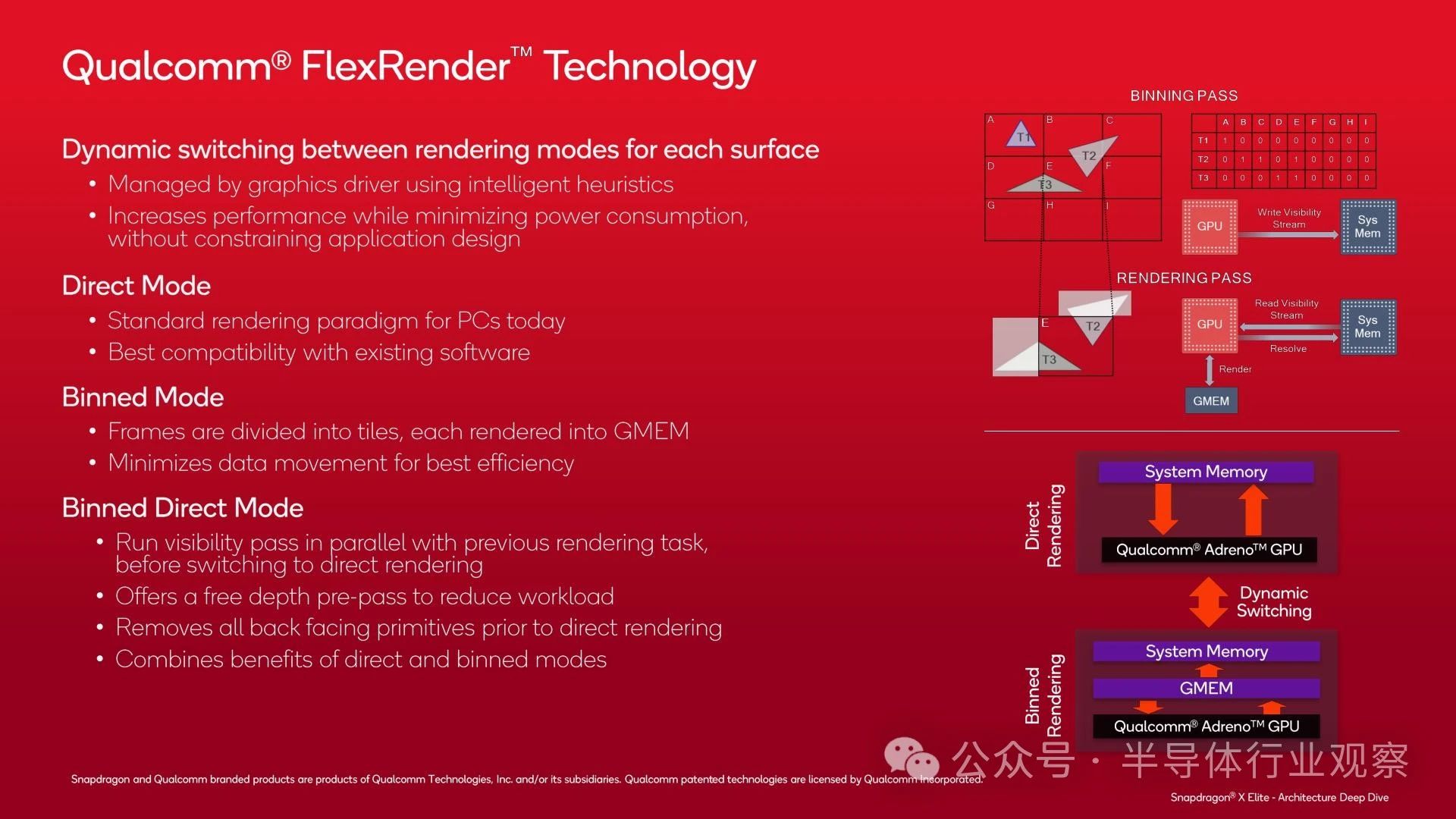
As mentioned earlier, Adreno X1 supports multiple rendering modes for optimal performance, which the company refers to as Flexrender technology. This is a less common theme in PC GPU design, but due to historical and efficiency reasons, it is more important in the mobile field.
In addition to traditional direct/instant mode rendering methods (typical of most PC GPUs), Qualcomm also supports block based rendering, which they refer to as merge mode. Like other block based renderers, merge mode divides the screen into multiple blocks and renders each block separately. This allows the GPU to process only a portion of the data at once, store the majority of the data in its local cache, and minimize the flow of traffic to DRAM, which consumes power and limits performance.
Finally, Adreno X1 has a third mode that combines the advantages of split box rendering and direct rendering, which they refer to as split box direct mode. This mode runs the sub box visibility channel before switching to direct rendering, as a means of further removing back (invisible) triangles so that they are not rasterized. Only after removing these data will the GPU switch to direct rendering mode, and now the workload has been reduced.
The key to ensuring the normal operation of graded rendering mode is the GMEM of the GPU, which is a 3MB SRAM block that can serve as a high bandwidth register for the GPU. Architecturally speaking, GMEM is not just a cache because it is separated from the system memory hierarchy, and the GPU can perform almost any operation on memory (including using it as a cache when necessary).
The size of the GMEM block is 3MB, which is not very large overall. But it is enough to store a tile, thus preventing a large amount of traffic from impacting system memory. And its speed is also very fast, with a bandwidth of 2.3TB/s, which is enough to allow ROP to run at full speed without being limited by memory bandwidth.
With the GMEM block, in an ideal scenario, the GPU only needs to write data to DRAM once for each work when rendering the block. Of course, in practice, DRAM traffic may be higher than this, but this is one of Qualcomm's key features to avoid GPUs writing data to DRAM and occupying memory bandwidth and power.
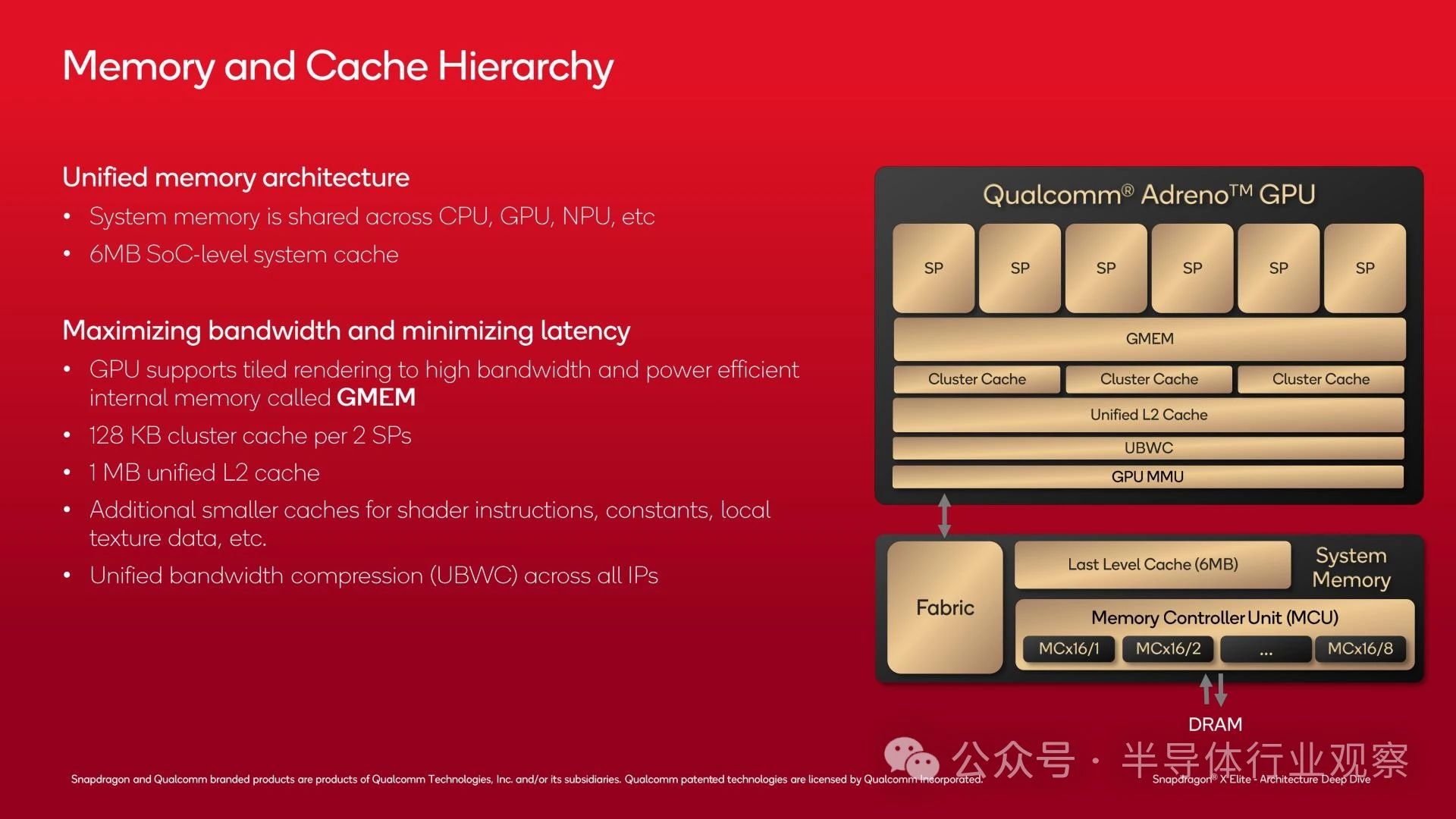
When Adreno X1 really needs to enter system memory, it will go through its remaining cache and finally reach the shared memory controller of Snapdragon X.
On top of GMEM, each pair of SPs has a 128KB cluster cache (for a complete Snapdragon X, there is a total of 384KB). On top of this, there is also a 1MB GPU unified L2 cache.
Finally, the remaining system level cache (L3/SLC) serves all processing blocks on the GPU. When all other methods fail, there is also DRAM.
Finally, it is worth noting that the Adreno X1 GPU also includes a dedicated RISC controller within the GPU, which serves as the GPU Management Unit (GMU). The GMU provides multiple functions, among which the most important is power management within the GPU. The GMU collaborates with power management requests from other parts of the SoC, allowing the chip to redistribute power between different blocks based on the optimal performance allocation method determined by the SoC.
Performance and preliminary ideas
Finally, before concluding this in-depth analysis of the architecture, let's take a look at a few performance slides from Qualcomm. Although the performance of Snapdragon X will be visible to the world when retail devices are released next week, it has given us a better understanding of expected results before that. But it must be treated with caution.

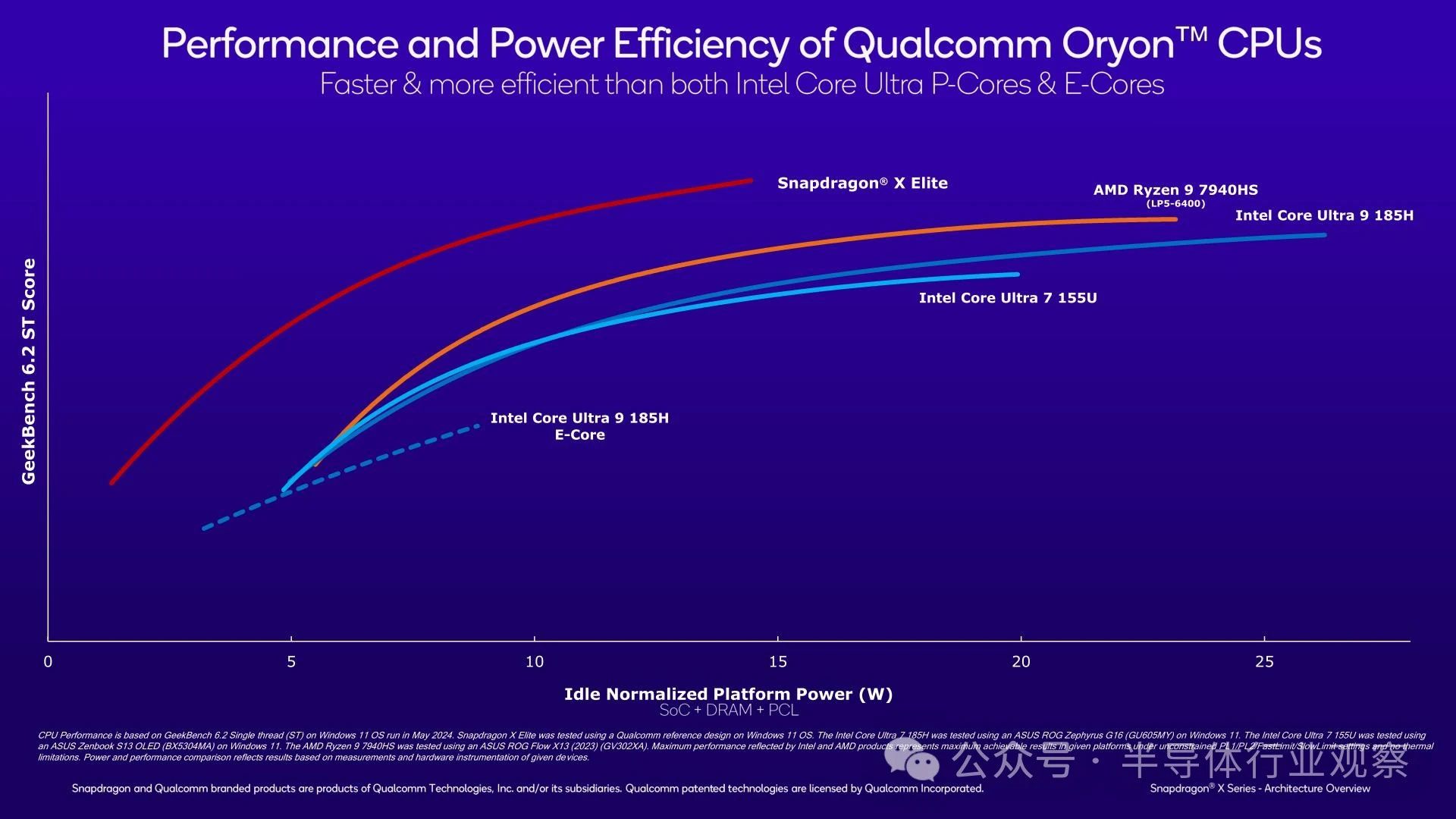
In terms of CPU, Qualcomm claims that Snapdragon X Elite can defeat all contemporary PC competitors in GeekBench 6.2 single threaded testing. Moreover, when considering energy efficiency, its leading advantage is also quite significant.
In short, Qualcomm claims that even if the TDP of x86 cores is not limited, the Oryon CPU core in Snapdragon X Elite can still outperform Redwood Cove (Meteor Lake) and Zen 4 (Phoenix) in absolute performance. Given that the acceleration of mobile x86 chips can reach up to 5GHz, this is a bold statement, but it is not impossible.
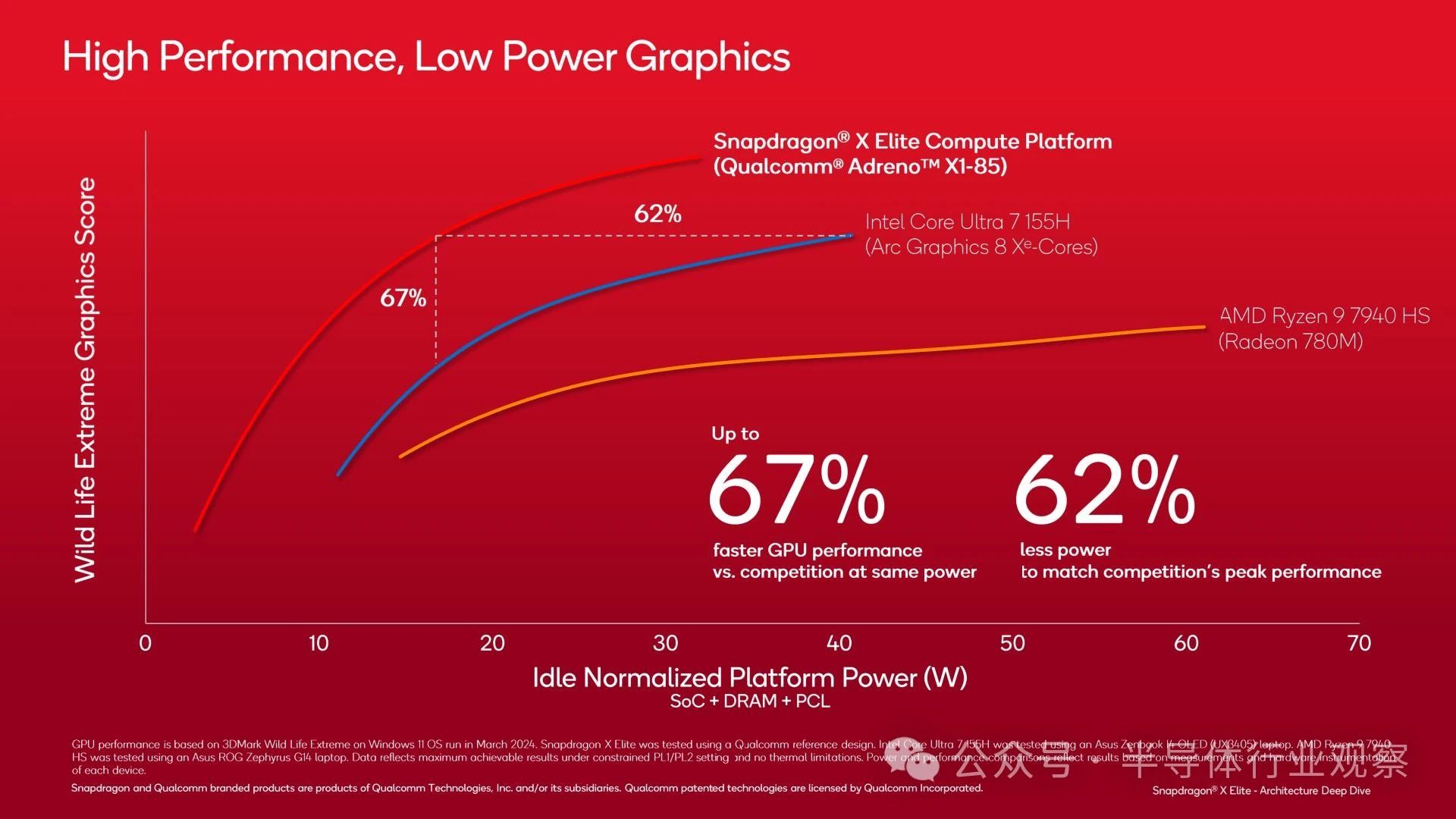
At the same time, Qualcomm has also achieved similar energy efficiency improvements in GPUs. However, the discussed workload 3DMark WildLife Extreme is unlikely to translate into most games, as it is a benchmark focused on mobile devices and has been repeatedly optimized in the drivers of each mobile SoC vendor for a long time.
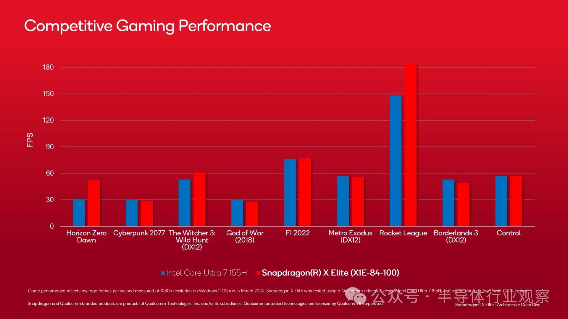
Performance benchmarking using actual games may be more useful here. Although Qualcomm may be selecting some good products, the top Snapdragon X SKU often competes with Intel's Core Ultra 7 155H. It is undeniable that its overall performance is not impressive, but it is gratifying to see Qualcomm's current performance in real-world games. In this situation, even a draw/defeat that is just one of Intel's better mobile chips is not bad.
Preliminary ideas
The above is our first in-depth study of the Qualcomm Snapdragon X SoC architecture. Qualcomm will invest in the Windows on Arm ecosystem for the long term, hoping to become the first of many ecosystems as the company seeks to become the third largest Windows CPU/SOC supplier.
But the ultimate significance of Snapdragon X SoC and its Oryon CPU core is not just as a SoC for laptops. Even though Qualcomm has achieved great success in this area, the number of PC chips they ship is only a drop in the bucket compared to their true strength foundation in the Android SoC field. And Oryon will illuminate the path of significant transformation for Qualcomm Mobile SoC here.
As Qualcomm has pointed out since the beginning of its Oryon journey, this will ultimately become the core CPU core of all Qualcomm products. Starting from this month, the PC SoC will eventually expand to include mobile SoCs such as Snapdragon 8 series, and further on, it will also include high-end branches such as Qualcomm's automotive products and XR earphone SoCs. Although I doubt whether we will really see Oryon and its successors in Qualcomm's products from top to bottom (the company needs small and affordable CPU cores to support its budget product line, such as Snapdragon 6 and Snapdragon 4), there is no doubt that in the long run, it will become the cornerstone of most of their products. This is the differentiated value of manufacturing one's own CPU kernel - by using it in as many places as possible to obtain maximum value from the CPU kernel.
Ultimately, Qualcomm has been heavily promoting its next-generation PC SoC and its customized CPU core for the past 8 months, and now it's time to get all the components in place. The prospect of having a third competitor (and an Arm based competitor) in the PC CPU field is exciting, but slides and advertisements are not hardware and benchmarks. Therefore, we eagerly await what next week will bring and see if Qualcomm's engineering capabilities can fulfill the company's grand ambitions.


