Electric drive inverters are widely recognized as the core components of hybrid and electric vehicles in the industry. From the initial tens of kilowatts to the current hundreds of kilowatts, their requirements for rated power are becoming increasingly high. Medium to high power inverters require a nominal current of several hundred to several thousand amperes for the power module. Only by parallelizing multiple bare chips, sometimes multiple sub modules (integrating multiple bare chips on the same packaging substrate), or even multiple power modules, can such high currents be achieved [1].
In this case, weight, size, and cost are the main factors that constrain the design of power modules. The three-phase half bridge inverter solution originally designed using IGBT has become very popular, and currently using higher performance silicon carbide power modules to design inverters is a new trend. Power module design is usually a trade-off and compromise between thermal and electrical performance. A well-designed power module can evenly distribute current between the upper and lower bridge arm switching tubes, as well as between the bare chips inside the switching tubes, provided that their static parameters do not differ significantly. In addition, a good circuit layout means that only when the mutual thermal effect between bare chips is reasonable, can the distribution of thermal stress be balanced.
This article introduces the development steps and process of a temperature measurement system for continuous operation of an electric drive inverter module, and analyzes the thermal imbalance phenomenon between parallel silicon carbide wafers that affects the service life of the power module. Parasitic components and static parameters (such as on state resistance and threshold voltage) caused by circuit layout are the main factors causing thermal imbalance in parallel devices. In paper [2], the asymmetry of circuit layout is discussed in detail, which can affect the gate to source loop, cause series inductance, and lead to mismatch in the drive loop, thereby seriously affecting the dynamic performance of parallel devices.
The paper [3] describes how to analyze the thermal imbalance problem of the power module in steady-state through infrared thermal imaging. Although the distribution range of on state resistance is an important static parameter, the relationship between resistance and temperature will compensate for the distribution range of on state resistance. In fact, heating up the chip will alleviate the thermal imbalance caused by the natural distribution range of leakage source on state resistance.
This article will focus on another key parameter: threshold voltage (Vth), which has a significant impact on the conduction and turn off performance of the switch, thereby affecting the energy loss of the power switch. The difference in threshold voltage Vth between two parallel chips can lead to energy imbalance, ultimately affecting the performance of the entire power module. The paper [4] provides a detailed description of the impact of Vth on switch energy consumption, demonstrating that when Vth increases by 500mV, the dissipation power in the conduction state may increase by up to 40%.
Based on this argument, we believe it is necessary to establish a temperature measurement system that can directly measure the switch temperature under normal working conditions to evaluate and characterize the heat dissipation performance of different bare chips within the power module. Not only do we strive to minimize the distribution range of process parameters on the production line, including the distribution range of threshold pressure Vth, but we also need to take further improvement actions at the module assembly level based on the small differences between the two closest chips within the module. We used this concept to assemble two different power modules: the first module is called GAP1, with a maximum distribution range of internal bare chip threshold voltage Vth of 250mV (around the average value+/-125mV), and the second module is called GAP2, with a maximum variation range of Vth of 500mV (around the average value+/-250mV). Two different switching frequencies were used for testing: the typical operating frequencies of the electric drive inverter are 8kHz and 12kHz. As is well known, the increase in dissipated power is directly proportional to the switching frequency.
A. Experimental setup
Our main goal is to design and develop a temperature measurement system that enables us to measure the temperature of power chips in practical application environments closer to electric drive inverters. Therefore, it is necessary to start with suitable mechanical components as well as hydraulic, electrical, and electronic components, so that all components are directed towards the above goals. The following diagram is the block diagram of the final temperature testing system that has been implemented.
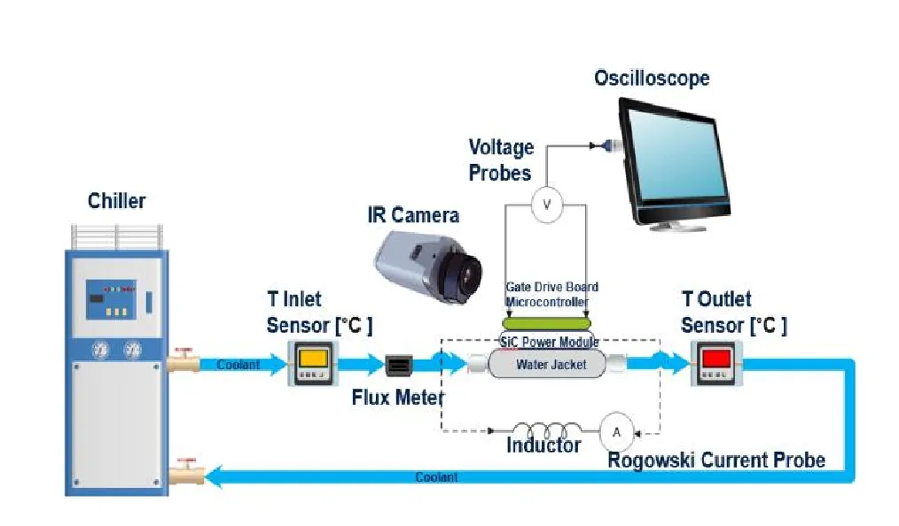
▲Figure 1: Complete Temperature Measurement System - Block Diagram
The hydraulic part of the temperature measurement system consists of a chiller, an inlet valve, and an outlet valve. The coolant circulates in the hydraulic pipeline to dissipate heat for the temperature measurement device. The temperature and flow rate of the inlet valve, as well as the appearance size of the water jacket (water tank), are important parameters that determine the size of the inverter, as they directly affect the RTH thermal resistance of the package. The coolant is a 50% -50% mixture of ethylene glycol and water, which is a common method for preparing coolant in variable frequency cooler circuits. In order to measure the flow rate of coolant, a flow meter is connected in front of the temperature measuring device. In our experiment, the coolant flow rate is set to 3.7 liters per minute. Using a thermometer to detect when the coolant temperature of the power module inlet valve reaches the reference temperature of 65 ℃. The aluminum heat sink dissipates heat for the power module, and the gate signal of the power module is provided by a dedicated gate drive board. Figure 2 shows the temperature measurement experiment setup.
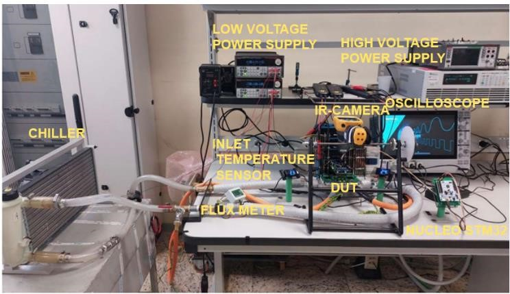
▲Figure 2: Experimental setup
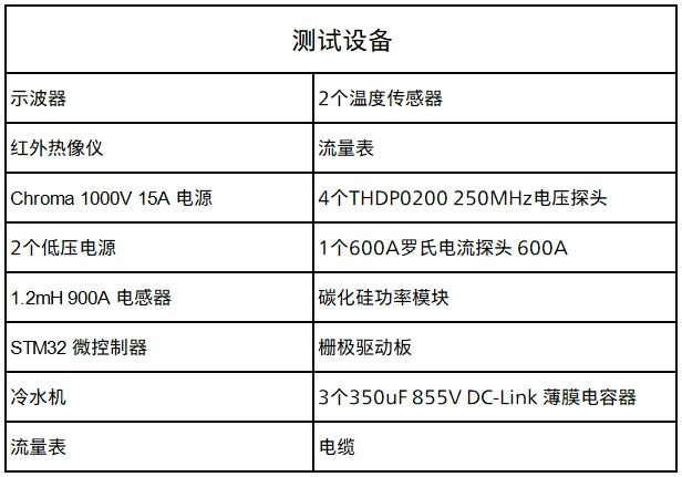
Here is the equipment list
Table 1: Testing Equipment
B. Design of temperature measuring equipment and gate driver board
We conducted thermal analysis on a continuous high-frequency operating silicon carbide three-phase power module. Especially, by disconnecting the middle bridge arm of the power module and connecting the AC terminals of bridge arm U and bridge arm W to a 1.2mH inductive load, a full bridge topology is obtained (Figure 3).
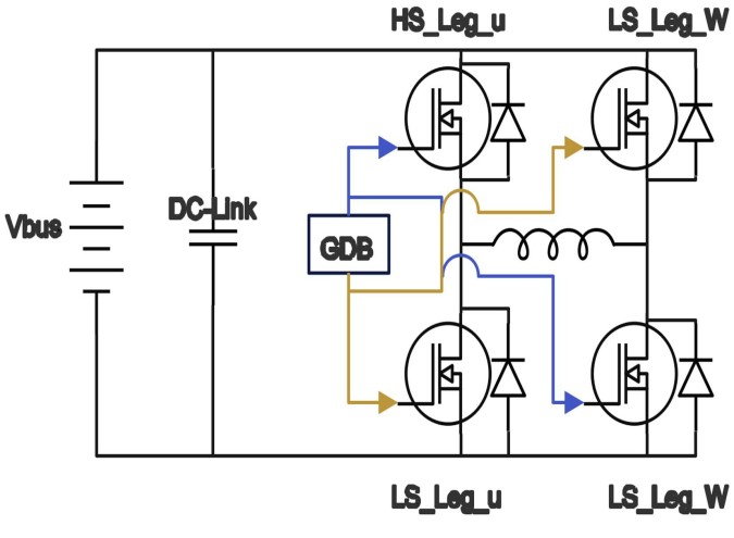
▲Figure 3: Half bridge equivalent circuit
How to implement the driver module through a multi-layer structure is a key factor to consider when developing temperature measurement systems. The first stage (power supply) uses a DC-DC boost converter to provide+18V and 5V voltage, which is the power supply required for switch operation. The second level (motherboard) includes a driver and a on/off resistor, which is used to drive charge injection into the gate source capacitor to avoid reaching the breakdown voltage of the device during the switching process. The following image shows the 3D models of these boards.
The final level is the control module implemented by the Nucleo STM32 microcontroller board. This module adopts a unipolar PWM control method, driving switches on two diagonal lines with the same signal. The complementary signal and the required dead time are used to drive the power switch on the second diagonal. According to the load conditions and actual working conditions, set the duty cycle of the PWM signal to obtain a sinusoidal current waveform with a peak current that meets the design requirements. Figure 4 shows the relevant waveforms of PWM complementary signal and load current (460 A Imax).
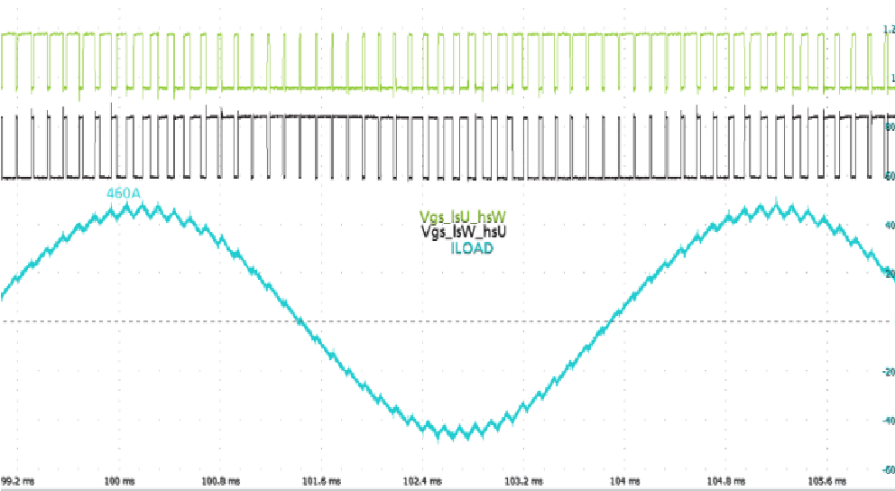
▲Figure 4: PWM drive signal and load current
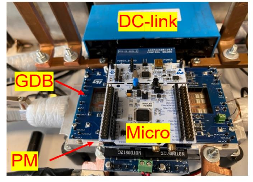
▲Figure 5: Gate Driver Board - Power Supply and Main Board
The gate drive board is installed on top of the power module, as shown in the above figure. The two boards have a pyramid shaped and complementary structure, which are inserted together through pins to minimize wiring distance, parasitic components on the drive board, and signal propagation delay.
In the following figure, you can see the testing tools used, as well as the DC bus and microcontroller board. Because high-frequency current flows through the busbar, special attention should be paid to the correct size of the busbar during the design phase. There are two openings on the board for us to directly observe the tested chip and measure the junction temperature (TJ) using an infrared thermal imager.
▲Figure 6: Electrical System Overview
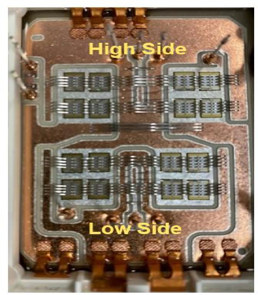
The characteristics of the measured SiC power module are as follows: at 25 ℃, the typical on state resistance value RdsON=1.9m Ω (for each switch), the nominal current Iphase=340A, and the breakdown voltage Vb=1200V. Figure 7 shows one bridge arm of the full bridge converter: each switch is composed of eight parallel bare chips. In the following figure, we can see the internal circuit layout of the temperature measuring device and determine the positions of the eight bare chips that make up the upper and lower bridge arm switches.
▲Figure 7: Layout of the tested device circuit
C. The effect of threshold pressure difference between parallel chips on temperature imbalance
The test voltage and current are 400V bus voltage and 200Hz 340 Arms sine phase current, respectively. The thermal imbalance phenomenon is tested at different dissipated powers using two switching frequencies of 8kHz and 12kHz [3].
The purpose of temperature measurement is to quantify the temperature difference between the highest and lowest temperature chips in the 32 full bridge chips, and compare the heat dissipation performance of GAP 1 module and GAP 2 module under the same switching frequency conditions.
It is worth mentioning that in order to achieve the required measurement accuracy of the experimental device, a pre characterization measurement process was carried out on the FLIR E-76 thermal imager. The main parameters involved include the installation position angle and the emission coefficient related to the surface material and external light conditions. Calibrate the power module by heating it with a hot plate within the steady-state temperature range of 50 ° C to 175 ° C. Finally, check the NTC reading against the set value of the hot plate temperature to ensure consistency between the two.
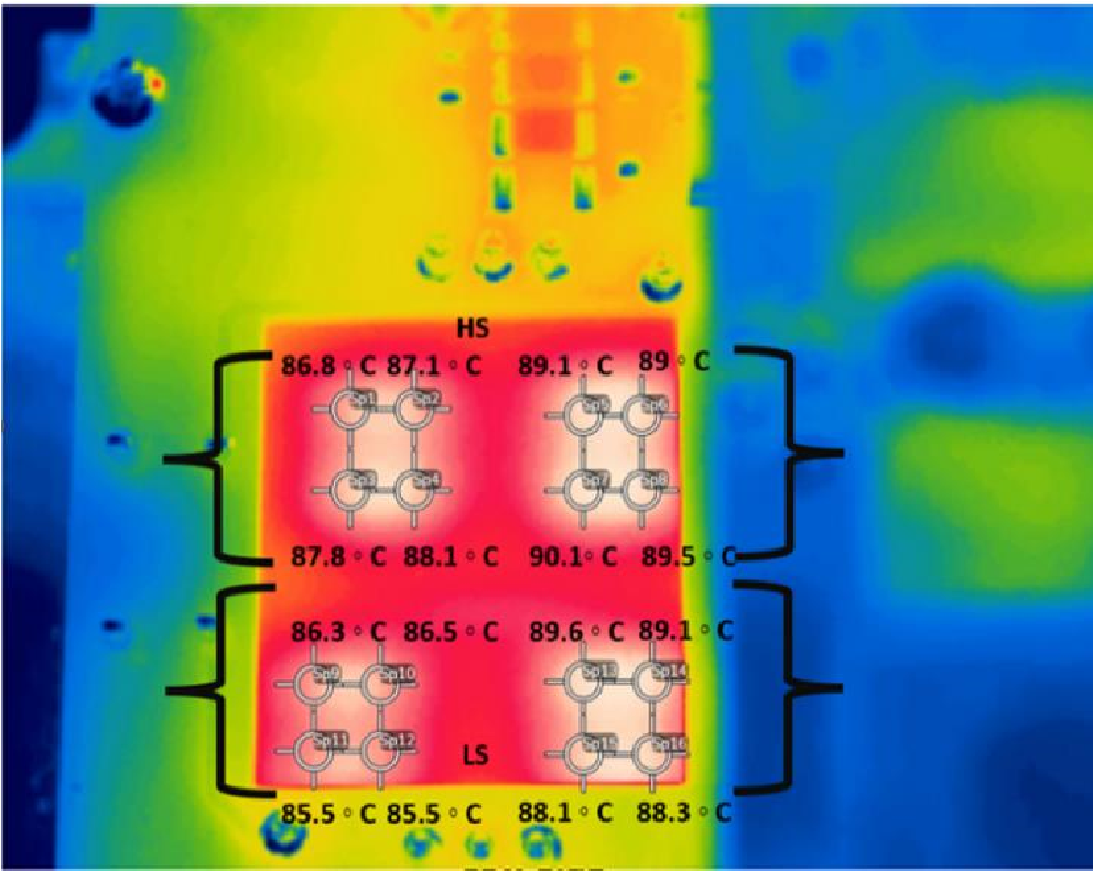
Only after completing the calibration of the experimental device can thermal imaging begin. Figures 8 and 9 show the infrared thermal images of the GAP 1 module at a switching frequency of 12kHz, along with the measured junction temperature values for each chip inside the switch.
The following image shows the infrared thermal image of the bridge arm W at a switching frequency of 12 kHz.

▲Figure 9: Infrared thermal image of bridge arm W at 12kHz
Perform the same temperature measurement experiment on the GAP 2 module. The eight bare pieces above belong to the upper bridge arm switch, while the eight bare pieces below belong to the lower bridge arm switch. Temperature analysis was conducted on GAP 1 module and GAP 2 module under switching frequency conditions of 8kHz and 12kHz, respectively. The table below summarizes the measurement analysis results and reports the maximum and minimum temperatures measured at each step.
Table 2: Test Results

In the GAP 1 module, the temperature difference between the highest and lowest chips is 4.4 ° C at 8kHz and 4.6 ° C at 12kHz. In selecting the GAP 2 module for Vth based on the selection criteria, the thermal increment is 6.3 ° C at 8kHz and 8.7 ° C at 12kHz.
D. Conclusion
Tests have shown that reducing the threshold pressure difference of parallel silicon carbide chips can greatly reduce the temperature difference between chips. In addition, as the switching frequency increases, the method of reducing the temperature difference by reducing the bare chip threshold pressure difference becomes more effective. In particular, during testing, the temperature difference decreased by 25% at 8kHz and nearly 50% at a switching frequency of 12kHz. The factors that cause switch dissipation power include Eon, Eoff, diode reverse recovery loss, and of course, switch frequency.
From the experimental results, it can be seen that for the given selection criteria, increasing the switching frequency to reduce temperature difference is not as effective as reducing the range of threshold voltage distribution. Due to many technical issues during the measurement process, including bus overheating and power supply voltage ripple, it is not possible to perform tests at the typical nominal battery voltage of the previous generation of electric vehicles. It is expected that this will expand the temperature difference, therefore, starting from the selection criteria or device threshold pressure range, a mathematical model that can predict junction temperature thermal imbalance will be very helpful.

