TVS Transient Voltage Suppressor Diode is a semiconductor device designed specifically to suppress transient overvoltages in circuits, such as electrostatic discharge (ESD), lightning induction, power surges, etc. Its core function is to safely discharge transient energy and protect sensitive components (such as chips and sensors) from high voltage impact through rapid conduction and clamping voltage. Here are the technical details and application analysis:
1、 Core working principle
Transient threat sources
Nanosecond high voltage pulses generated by lightning induction, power switch switching, electrostatic discharge (ESD), etc. (typical waveform: 8/20 μ s surge pulse defined by IEC 61000-4-5 standard).
protection mechanism
Avalanche effect: When the voltage exceeds the breakdown voltage (Vbr), the TVS instantly conducts, clamping the voltage within a safe range.
Fast response: Picosecond level response time (usually<1ps), much faster than gas discharge tubes or varistors.
Voltage clamp: Limit the voltage to the rated clamp voltage (Vc) to avoid damage from overvoltage in the subsequent circuit.
Mainstream types and packaging
Unidirectional TVS
Structure: A single PN junction that only protects against unipolar pulses.
Application: Single pole protection scenarios such as power cords and battery interfaces.
Bidirectional TVS
Structure: Two reverse parallel PN junctions to protect against positive and negative pulses.
Application: Bipolar signal interfaces such as USB, HDMI, antenna, etc.
Array TVS
Structure: Multi channel integrated packaging (such as 4-channel, 8-channel).
Advantages: Save PCB space and provide unified protection for multiple signals (such as the 8 wires of Ethernet interfaces).
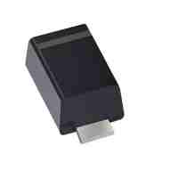
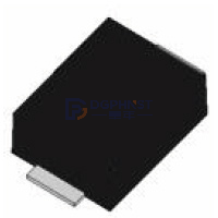
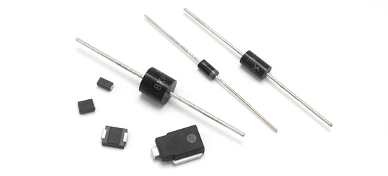
Packaging form
SOT-23: Universal packaging, suitable for single channel protection.
DFN/QFN: Ultra small package (such as 1.0mm × 0.6mm), suitable for high-density PCBs.
DO-218AB (SMC): High power package, suitable for power modules.
4、 Typical application scenarios
Consumer Electronics
Example: Mobile phone charging port (USB-C), LCD screen backlight driver, camera module.
Selection: Low capacitance (<1pF) bidirectional TVS, such as Littelfuse SP3012 series.
Automotive Electronics
Examples: CAN bus, in car entertainment system, ADAS sensor interface.
Requirement: Passed AEC-Q101 certification, high temperature resistance (-55 ℃~+175 ℃).
Industrial control
Example: RS-485 interface, PLC input/output ports, frequency converter drive circuit.
Selection: High power TVS (such as 1500W PPP), such as Vishay SMBJ series.
communication devices
Example: Fiber optic module, base station power supply, Ethernet interface.
Key parameters: Low insertion loss (<0.5dB), compatible with high-speed signals (such as 10Gbps).
5、 Core steps for selection
Determine the protective voltage
Select the breakdown voltage (Vbr) based on the operating voltage (VCC) of the protected circuit, usually Vbr=1.1 × VCC.
Example: Choose the 6V Vbr model for a 5V system.
Evaluate signal rate
High speed interfaces (such as USB 3.0, HDMI 2.1) require the selection of ultra-low capacitance models (<0.5pF).
Formula: The signal attenuation caused by capacitance Δ V=I × C × Δ t, ensuring that Δ V<5% × Vswing.
Match surge level
Select surge resistance level according to IEC 61000-4-5 standard:
Level I lightning protection: 6kV (line to ground)/3kV (line to line).
Level II lightning protection: 4kV (line to ground)/2kV (line to line).
Level III lightning protection: 2kV (line to ground)/1kV (line to line).
Thermal Design and Reliability
Calculate power dissipation: P=Vclamp × Ipeak × tpulse, ensuring that it is lower than the rated PPP of TVS.
Choose certified models (such as UL, VDE, AEC-Q101).