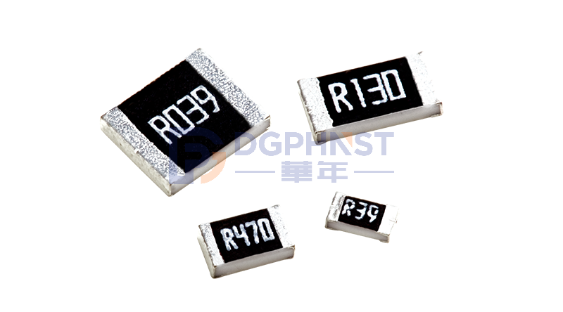
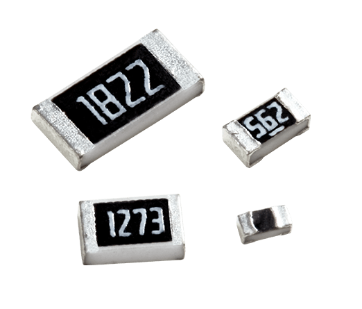
The densely packed surface mount resistors on the motherboard are the basic components for voltage division, current limitation, and impedance matching in electronic circuits. As the most widely used and cost-effective passive component in PCB boards, thick film surface mount resistors have captured more than 90% of the general resistor market share in consumer, industrial control, and automotive electronics.
The surface mount resistor, which is small in size, contains a multi-layered precision composite structure internally. Today, we will disassemble the internal structure of the thick film resistor layer by layer with the help of images.
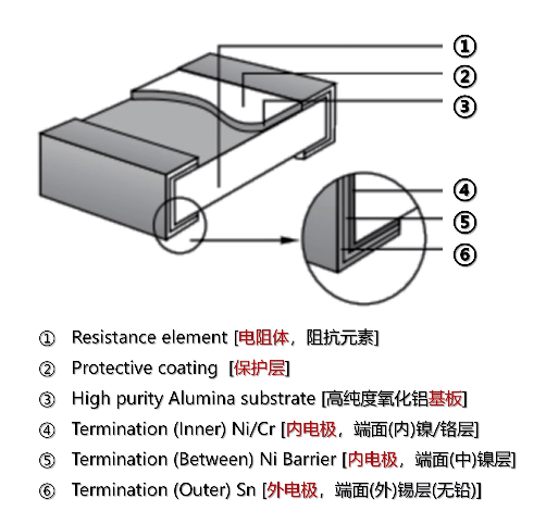
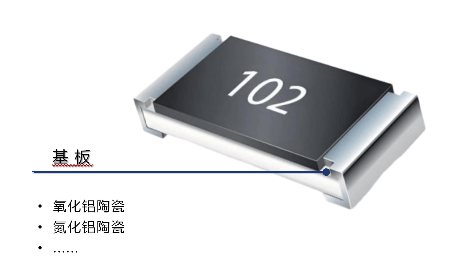
Overall View: Classic "Sandwich" Layer Structure
Standard thick film surface mount resistors use a standardized layered design from top to bottom, forming a four-layer composite structure. From bottom to top, they are arranged as follows: high-purity aluminum oxide substrate → resistor functional layer → inner and outer electrodes → protective coating. The structure is compact and sintered into one piece.
Layer-by-Layer Dissection | Four Core Structures + Materials
1. Substrate: Insulating Support Frame of the Resistor
The substrate is the physical carrier and insulating base of the entire resistor, carrying all functional film layers and also serving as the core heat dissipation carrier. Industry material requirements include high insulation, high mechanical strength, high thermal stability, and excellent thermal conductivity.
Comparison of Two Main Substrate Materials
- Aluminum Oxide Ceramic (Mainstream in the Market): It offers a perfect balance between cost-effectiveness, thermal conductivity, insulation, and mechanical performance, suitable for most consumer electronics and industrial control circuits. It has low mass production costs and is the standard substrate material for general thick film resistors.
- Aluminum Nitride Ceramic (High-End Model): Its thermal conductivity far exceeds that of aluminum oxide ceramic, offering maximum heat dissipation capabilities, specifically targeting high-power circuits, high-density automotive power supplies, and industrial high-frequency equipment. However, its raw materials and sintering costs are very high.
2. Resistor Body: Core Functional Layer of the Resistor
The resistor body is the core layer that determines the resistance value, accuracy, temperature coefficient (TCR), and heat resistance of the resistor. It is a unique thick film sintered coating, and its material directly determines the upper limit of the electrical parameters of the component.
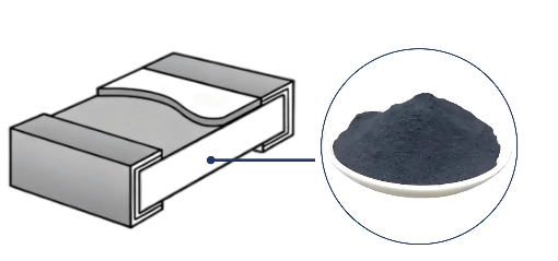
Three Categories of Materials
- Oxides of Ruthenium (Industry Mainstream): The preferred material for general surface mount resistors, with excellent performance stability and TCR. It mainly consists of ruthenium dioxide, bismuth ruthenate, and lead ruthenate, suitable for resistors with 1% and 5% conventional accuracy, with controllable mass production costs.
- Base Metal Series: Focuses on cost reduction, suitable for low-end civilian cheap circuits, but with weaker temperature drift and accuracy performance.
- Polymer Thick Film: Flexible adaptation and strong anti-bending capability, often used in special flexible circuit board applications.
3. Composite Electrode Layer: Bridge for Circuit Conduction
The electrode connects the resistor body to the PCB circuit board, consisting of three-layer end structures: inner, middle, and outer. It meets multiple requirements including conductivity, oxidation resistance, solderability, and peeling resistance, with clear division of labor among layers.
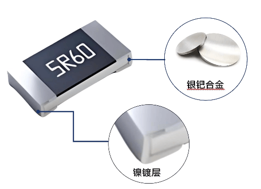
① Inner Electrode (Base Conductive Layer)
It adheres to both ends of the resistor body, responsible for current transmission. Commonly used materials include silver-palladium alloy (industry standard), pure silver (best conductivity), palladium-gold/platinum (high-end precision resistors), and pure copper (low-cost alternative).
② Middle Nickel Isolation Layer
It isolates the inner precious metal from the outer solder, preventing metal migration and protecting against plating corrosion, thus enhancing electrode life and welding reliability.
③ Outer Lead-Free Tin Plating Layer
It is the surface solderable plating layer, suitable for SMT surface mount reflow soldering process, meeting industry lead-free environmental standards, with good oxidation resistance and easy solderability.
4. Protective Layer: Armor for the Component
It fully covers the resistor body surface, isolating it from moisture, dust, acid-base chemical corrosion, while also resisting friction and mechanical damage, preventing oxidation and resistance value drift failure of the resistor body.
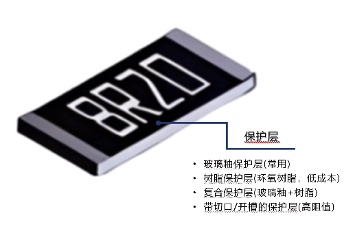
Four Types of Protective Layer Materials & Suitable Scenarios
① Glass Enamel Protective Layer (Most Common): It has high heat resistance, corrosion resistance, and strong insulation, and is standard for general industrial and automotive resistors.
② Resin Protective Layer: Made of epoxy resin, it has a simple process and extremely low cost, suitable only for low-end consumer electronics.
③ Composite Protective Layer: A double-layer combination of glass enamel and resin, combining high heat resistance and impact resistance, preferred for harsh working conditions.
④ Groove/Notch Protective Layer: Customized for high-resistance thick film resistors, optimizing resistance accuracy and avoiding high-voltage breakdown risks.
Conclusion
In summary, the core design principle of the thick film resistor is: the substrate supports and insulates, the resistor body realizes the electrical performance, the electrode completes the circuit conduction, and the protective layer isolates external damage, each fulfilling their respective roles to ensure long-term stability of the resistor.
A surface mount resistor with a size only at the millimeter level, from the ceramic base to the micrometer-level precision film layer, every part contains precise material ratios and manufacturing processes. Understanding the internal construction logic can significantly improve efficiency and avoid detours in component selection matching, circuit fault maintenance, and supply chain material cost optimization.