In the early days, we all built our own power supply circuits, and now there are many integrated chips. DC-DC circuits are also ubiquitous in electronic products. This article shares some basic knowledge of DCDC circuit design with everyone.
Concept and characteristics
DC-DC refers to a direct current to direct current power supply. It is a device that converts electrical energy from one voltage value into electrical energy from another voltage value in a DC circuit.
For example, if a converter can convert a DC voltage (5.0V) into other DC voltages (1.5V or 12.0V), we call this converter a DC-DC converter, or a switching power supply or switch regulator.
DC-DC converters generally consist of control chips, inductor coils, diodes, transistors, and capacitors.
When discussing the performance of DC-DC converters, it is not possible to judge their superiority or inferiority solely based on the control chip. The characteristics of its peripheral circuit components and the wiring method of the substrate can change the performance of the power circuit, therefore, comprehensive judgment should be made.
The use of DC-DC converters is beneficial for simplifying power circuit design, shortening development cycles, achieving optimal performance, and is widely used in communication fields such as power electronics, military industry, scientific research, industrial control equipment, communication equipment, instrumentation, switching equipment, access equipment, mobile communication, routers, as well as industrial control, automotive electronics, aerospace, and other fields.
With high reliability and easy system upgrades, the application of power modules is becoming increasingly widespread. In addition, DC-DC converters are widely used in products such as mobile phones, MP3 players, digital cameras, and portable media players. In terms of circuit type classification, it belongs to chopper circuits.
Its main characteristic is high efficiency: compared with the LDO of linear regulators, high efficiency is a significant advantage of DC-DC. Usually, the efficiency is above 70%, and the high efficiency can reach over 95%. Secondly, it adapts to a wide voltage range.
Modulation method:
1. PFM (Pulse Frequency Modulation)
The switching pulse width is constant, and by changing the frequency of the pulse output, the output voltage is stabilized. The PFM control type has the advantage of low power consumption even when used for a long time, especially under small loads.
2. PWM (Pulse Width Modulation)
The frequency of the switch pulse is constant, and by changing the pulse output width, the output voltage is stabilized. PWM control has high efficiency and good output voltage ripple and noise.
In general, the performance differences of DC-DC converters using two different modulation methods, PFM and PWM, are as follows:
The frequency of PWM and the selection method of PFM duty cycle. When the PWM/PFM conversion type is used for small loads, PFM control is implemented, and it automatically switches to PWM control during heavy loads.
Architecture classification
There are three common principles and architectures for DC-DC:
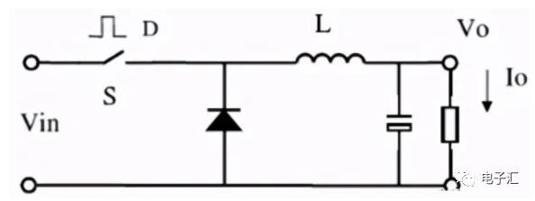
1. Buck (buck type DC/DC converter)
2. Boost (Boost type DC/DC converter)
3. Buck Boost (Boost Boost DC/DC Converter)

Design skills and requirements for selecting main technical parameters
The design of DC-DC circuits should at least consider the following conditions:
The range of external input power supply voltage and the magnitude of output current.
The maximum voltage, current, and system power output by DC-DC.
1. Input/output voltage
Choose according to the recommended operating voltage range of the device, and consider the actual voltage fluctuation range to ensure that it does not exceed the device specifications.
2. Output current
The continuous output current capability of the device is an important parameter, which should be referred to when selecting, and a certain margin should be retained.
The selection of this parameter also needs to evaluate the instantaneous peak current and heat generation of the circuit, comprehensively determine it, and meet the derating requirements.
3. Ripple
Ripple is an important parameter for measuring the output voltage fluctuation of a circuit. Pay attention to the ripple of light and heavy loads, and generally, the ripple of light loads should be larger. Pay attention to whether light load ripple will exceed the requirements in situations such as nuclear power. Actual testing under various scenario loads. Usually, a 20M bandwidth oscilloscope is used for testing.
4. Efficiency
Pay attention to both light and heavy loads simultaneously. Light loads can affect standby power, while heavy loads can affect temperature rise. Usually, the efficiency of 10mA under 12V input and 5V output is generally over 80%.
5. Transient response
The transient response characteristics reflect whether the system can adjust in a timely manner to ensure the stability of the output voltage when the load changes dramatically. The requirement is that the output voltage fluctuation should be as small as possible, generally below 10% of the peak to peak value.
In practice, it is important to choose feedback capacitors according to the recommended values. The common values range from 22p to 120pF.

6. Switching frequency
The commonly used switching frequency is mostly above 500kHz. There are also products with higher switching frequencies ranging from 1.2M to 2M. Due to the increased switching losses at higher frequencies, the IC's heat dissipation design is better, so it is mainly concentrated in products with low input current of 5V low-voltage. The switching frequency is related to the selection of inductors and capacitors, and other issues such as EMC and noise under light loads are also related to it.
7. Feedback reference voltage and accuracy
The feedback voltage should be compared with the internal reference voltage, combined with the external feedback voltage divider, to output different voltages. The reference voltage of different products may vary, such as 0.6~0.8V. When replacing, pay attention to adjusting the feedback resistance.
The feedback resistor should be selected with a precision of 1%, as long as it is recommended by the manufacturer. Generally, it should not be selected too large to avoid affecting stability.
The accuracy of the reference voltage affects the accuracy of the output. The common accuracy is below 2%, such as 1%~1.5%. The cost of products with high accuracy may vary. Choose as needed.
8. Linear stability and load stability
Linear stability reflects the stability of input voltage changes and output voltage. Load stability reflects the stability of output voltage due to changes in output load. The general requirement is 1%, and the maximum should not exceed 3%.
9. EN level
The high and low levels of EN must meet the requirements of device specifications, and some ICs cannot exceed a specific voltage range; When dividing the resistance voltage, attention should be paid to timely turning off, and the maximum range of voltage fluctuation should be considered.
Due to the need for timing control, this pin will add a capacitor. In order to adjust the level and turn off the discharge, there should also be a resistance to ground.
10. Protection performance
There should be overcurrent protection OCP, overheating protection OTP, etc., and the protection should be able to self recover after the condition disappears.
11. Others
Require soft start; Thermal resistance and packaging; The temperature range should cover high and low temperatures.
General principles for device selection
Universality
High cost performance ratio
Easy procurement has a long lifecycle
Compatibility and substitutability
Resource conservation
Derating
Easy production and normalization
Requirements for selecting peripheral devices
1. Input capacitance
To meet the requirements of voltage resistance and input ripple. The general withstand voltage requirement is 1.5 to 2 times or more of the input voltage. Note that the actual capacity of ceramic capacitors will decrease with the bias effect of DC voltage.
2. Output capacitance
To meet the requirements of voltage resistance and output ripple. General withstand voltage requirement of 1.5-2 times
The relationship between ripple and capacitance:
![]()
3. BST capacitor
Recommended values according to the specifications. Generally 0.1uF-1uF. The withstand voltage is generally higher than the input voltage.
4. Inductance
Different output voltages require different sensitivities; Note that the temperature rise and saturation current must meet the margin requirements, generally at least 1.2 times the maximum current (or the saturation current of the inductor must be greater than the maximum output current+0.5 * inductor ripple current). Usually, an appropriate inductance value L is chosen to ensure Δ IL accounts for 30% to 50% of the output current. Calculation formula:

5. VCC capacitor
According to the specifications, the value should not be reduced or too large, and attention should be paid to voltage resistance.
6. Feedback capacitance
According to the specifications, different manufacturers have different chip values and output voltage requirements.
7. Feedback resistor and EN voltage divider resistor
Require values to be taken according to the specifications, with an accuracy of 1%.
PCB design requirements
1. Place the input capacitor near the input Vin and power PGND of the chip to reduce the presence of parasitic inductance, as the noise caused by parasitic inductance due to discontinuous input current has a negative impact on the chip's voltage resistance and logic unit. Add a through-hole at the ground end of the capacitor to reduce impedance.
2. The power circuit should be as short and thick as possible, maintaining a small loop area and minimizing noise radiation. SW is a noise source that ensures current while keeping the area as small as possible, away from sensitive and easily disturbed locations. For example, the inductance is close to the SW pin and away from the feedback line. The output capacitor is close to the inductor, and a ground through-hole is added to the ground terminal.
3. VCC capacitors should be placed between the VCC pins of the chip and the signal ground of the chip, as close as possible, on the same layer without through holes.
4. FB is the most sensitive and susceptible part of the chip to interference, and is the most common cause of system instability.
Connect the FB resistor to the FB pin as short as possible and place it close to the IC to reduce noise coupling; The voltage divider resistor under FB is usually connected to the signal ground AGND;
Off noise source, SW, inductor, diode (asynchronous buck); FB wiring and grounding; The FB of the current load should be taken at the far end of the load, and the feedback capacitor wiring should be taken nearby.
5. The capacitance wiring of BST should be as short as possible and not too thin.
6. The heat dissipation of the chip should follow the design requirements and try to add through holes for heat dissipation at the bottom.