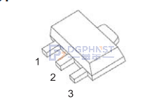
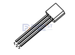
MOS transistor as a special driving circuit for switch transistor applications (commutation circuit)
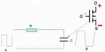
Compared with ordinary transistor, MOS transistor has many advantages. However, when applied as a high-power switch transistor, due to the capacitive input characteristics of MOS transistor, the input terminal of MOS transistor is equivalent to a small capacitor. The input switch excitation signal is actually in the process of repeatedly charging and discharging this capacitor. During the charging and discharging process, the MOS transistor conducts and closes with a lag, which slows down the process of "on" and "off", which is not allowed by the switching element (increased power consumption, burning out the switch transistor).
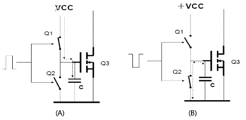
The voltage waveform becomes a distorted waveform of B, causing the switching transistor to malfunction and be damaged. The solution is that as long as R is small enough, or even without resistance, the excitation signal can provide sufficient current to quickly charge and discharge the equivalent capacitor. This way, the MOS switching transistor can quickly "turn on" and "off", ensuring normal operation. Due to the internal resistance of the excitation signal and the limited excitation current of the signal, we have added a "commutation circuit" to the input part of the MOS transistor as a switch to reduce internal resistance and increase excitation current to solve this problem, as shown in the following figure.
In the above figure, two switching transistors Q1 and Q2 are added between the gate S of MOS transistor Q3 used as a switch and the excitation signal. Both transistors are ordinary crystal transistors, connected in series. Q1 is an NPN type and Q2 is a PNP type, with the base connected together (actually a complementary emitter follower of PNP and NPN). The two transistors are equivalent to two switches that turn on alternately under the control of a square wave excitation signal, as shown in Figures A and B.
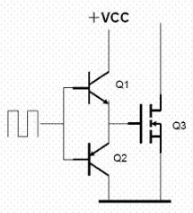
When the positive half cycle of the excitation square wave signal arrives; The transistor Q1 (NPN) is turned on and Q2 (PNP) is turned off. VCC charges the gate of MOS switch Q3 through Q1 conduction. Since Q1 is saturated conduction, VCC is equivalent to directly applying to the gate of MOS switch Q3. The instantaneous charging current is extremely high, and the charging time is extremely short, ensuring the rapid "on" of MOS switch Q3, as shown in Figure A (capacitor C in Figure A and Figure B is the equivalent capacitance of MOS switch gate S).
When the negative half cycle of the excitation square wave signal arrives; The transistor Q1 (NPN) is turned off and Q2 (PNP) is turned on. The charge charged at the gate of MOS switch Q3 is rapidly discharged through Q2. Due to Q2 being saturated and conducting, the discharge time is extremely short, ensuring the rapid "off" of MOS switch Q3, as shown in Figure B above.
Due to the limited current capacity of the gate S lead in the manufacturing process of MOS transistors, the instantaneous charging current of VCC to the gate S of the MOS transistor is huge when Q1 is saturated and conductive, which can easily damage the input terminal of the MOS transistor. In order to protect the safety of the MOS transistor, measures must be taken in the specific circuit to limit the instantaneous charging current value. An appropriate charging current limiting resistor R is connected in series in the gate charging circuit, as shown in Figure A below.
Selection of the resistance value of the charging current limiting resistor R; According to the size of the input capacitance of the MOS transistor, the frequency of the excitation pulse, and the size of the VCC (VCC is generally 12V) of the commutation circuit, it is generally determined to be between tens of milliohms and one hundred ohms.
Due to the increase of the charging current limiting resistor, the discharge speed when Q2 is turned on during the negative half cycle of the excitation square wave is limited (VCC generates current during charging, and VGS generated by the gate voltage during discharging, which is much smaller than VCC, and the presence of R greatly reduces the discharge rate), which deteriorates the switching characteristics of the MOS transistor. In order to ensure that the resistance value of R does not affect the rapid discharge rate during discharge, a diode D forming a discharge path is connected in parallel to the charging current limiting resistor R, as shown in Figure B above. This diode conducts during discharge and is reverse biased and cut off during charging. This increases the charging current limiting resistor and discharging diode, ensuring both the safety of the MOS transistor and the rapid action of its "on" and "off".
Another form of commutation circuit, the MOS transistor used in some low-power switching power supplies often adopts the circuit method shown in Figure A.
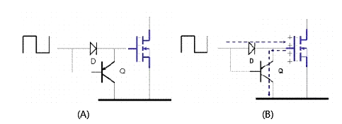
In the figure, D represents the charging diode and Q represents the discharging transistor (PNP). The working process is as follows: when the excitation square wave is in the positive half cycle, D is conductive, charging the equivalent capacitance of the MOS transistor input terminal (at this time, Q is cut off). When the excitation square wave is in the negative half cycle, D is cut off, Q is conductive, and the MOS transistor gate S is charged. Through Q discharge, the MOS transistor completes the "on" and "off" actions, as shown in Figure B. This circuit directly 'pours' the excitation signal, and the excitation signal source requires a low internal resistance. This circuit is generally applied to low-power switching power supplies.


