MOS switch applications must be equipped with a discharge resistor
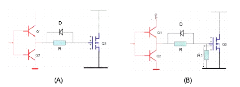
When the MOS transistor operates in the on/off state; Q1 and Q2 are alternately conductive, and the gate of the MOS transistor is in a state of repeated charging and discharging. If the power is turned off at this time, the gate of the MOS transistor has two states; One state is; Discharge state, the equivalent capacitance of the gate has no charge storage, and one state is; In the charging state, the equivalent capacitance of the gate is exactly in the fully charged state, as shown in Figure A.
Although the power is cut off, Q1 and Q2 are also in a disconnected state at this time, and the electric field at the gate of the MOS transistor still exists (which can be maintained for a long time), and the conditions for establishing a conductive channel have not disappeared. At the moment of restarting, due to the lack of established excitation signal, the drain power supply (VDS) of the MOS transistor is randomly provided. Under the action of the conductive channel, the MOS transistor immediately generates an uncontrolled huge drain current ID, causing it to burn out.
To avoid this phenomenon, a discharge resistor R1 is connected in parallel between the gate and source of the MOS transistor, as shown in Figure B. After shutdown, the stored charge in the gate is quickly released through R1. The resistance value of this resistor should not be too large to ensure the rapid release of the charge, usually around 5K to 10K.

The perfusion circuit is mainly designed for the capacitive input characteristics of MOS transistors when used as switch transistors, which cause hysteresis in the "on" and "off" actions. When MOS transistors are used for other purposes, it is used as a circuit; For applications such as linear amplification, there is no need to set up a perfusion circuit.

