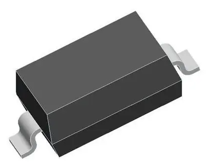
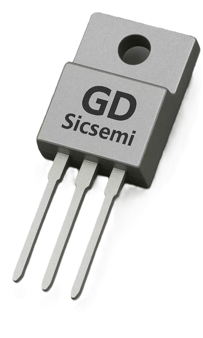
In a P-channel Enhanced Mode FET, VDS represents the voltage between the drain and source, while CGS represents the capacitance between the gate and source.
When calculating VDS, it is necessary to consider the working state of the P-Channel Enhanced Mode FET. Generally, the following formula can be used for calculation:
VDS = VDD – ID * RD
Among them, VDD represents the power supply voltage in the circuit, ID represents the drain current of the P-Channel Enhanced Mode FET, and RD represents the drain load resistance. This formula is based on Ohm's law and Kirchhoff's voltage law, and can be used to calculate VDS under different operating states.
When calculating CGS, it is necessary to consider the capacitance characteristics between the gate and source of the P-Channel Enhanced Mode FET. In general, the following formula can be used for calculation:
CGS = ε * A / d
Among them, ε represents the dielectric constant of the gate dielectric, A represents the gate area, and d represents the thickness of the gate dielectric. This formula is based on the definition formula of capacitance and can be used to calculate the CGS of P-Channel Enhanced Mode FET. It should be noted that in practical design, the capacitance between the gate and source of P-Channel Enhanced Mode FET is relatively small, so it can often be ignored.


