Inductors have alternating current, and laying copper at the bottom of the inductor will generate eddy currents on the ground plane. The eddy current effect will affect the inductance of the power inductor, and eddy currents will also increase system losses. At the same time, the noise generated by alternating current will increase the noise on the ground plane, which will affect the stability of other signals.
From the perspective of EMC, laying copper on the bottom of the inductor and a complete ground surface is beneficial for EMI design; The current production process of inductors has been upgraded, and shielded inductors are used. There are very few leaked magnetic induction lines, which have little impact on the inductance of the inductors and are also beneficial for heat dissipation.
How to choose in practical engineering?
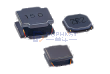
How to choose in engineering, the first step is to understand the structure of the inductor. We commonly use unshielded I-shaped inductors, semi shielded inductors, and integrated inductors. What are their characteristics?
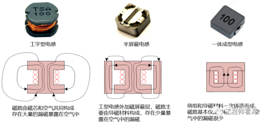
Unshielded I-shaped inductors are composed of magnetic cores and air, and their magnetic induction lines are completely exposed to the air without any magnetic shielding.
Half shielded inductor, as can be seen from its skeleton structure, has added magnetic shielding materials around the inductor on the basis of the I-shaped inductor. Due to the low magnetic resistance of magnetic shielding materials, the magnetic induction line is basically locked in the magnetic conducting material, and only a small part of the magnetic field will leak out from the air gap, so it can play a certain shielding role.
Integrated inductor is made by casting the winding and magnetic material in one go during the production of the inductor. There is only a small air gap inside to prevent saturation of the inductor, so there is basically no leakage of magnetic induction lines in this type of inductor.
The effect of unshielded I-shaped inductor and shielded inductor copper skin on inductance in the experiment.
The experiment found that under the condition of copper skin on unshielded I-shaped inductors, the inductance decreased, while shielded inductors had almost no effect.
What is the impact of copper plating on the bottom of the inductor on the power supply?
Before considering this issue, first review and understand the eddy current effect. The magnetic induction line ranges from N to S levels. When there is an alternating magnetic field passing through the surface of a conductor, according to the law of electromagnetic induction, an induced current is formed on the surface of the conductor, and the direction of the magnetic field generated by the induced current always plays a role in weakening the original magnetic field size.

Below is the current loop of the Boost boost DC/DC circuit, to discuss the impact of copper deposition at the bottom of the inductor on power supply design.
When Boost is working normally, the load current flows through the inductor, forming a loop. Due to the presence of switching tubes, the current is dynamically changing, which can form a magnetic induction line of the inductor. Some of the magnetic induction lines on the surface of the conductor form a closed magnetic circuit, and some of the magnetic circuits will form leakage magnetic flux and overflow into the air. If there is no copper coating at the bottom of the inductor, the magnetic flux lines that overflow from the inductor will exist in the entire power system, leaving no relatively quiet space for the system and causing a decrease in EMI performance.

If complete copper is applied to the bottom of the inductor, eddy current effect will be generated on the bottom plane of the inductor, which will cancel out the magnetic field generated by partial leakage inductance and weaken the original leakage magnetic induction line. The bottom of the inductor is coated with copper, and the eddy current generated is like an electromagnetic shielding cover, blocking the downward propagation of magnetic induction lines. Therefore, the high-frequency magnetic field generated by the inductor can be shielded on one side of the conductor, greatly reducing the impact of the high-frequency magnetic field on other components in space.

From two perspectives, from the perspective of EMI, it is recommended to apply copper; From the perspective of inductance, shielding inductance has no effect, so it is also recommended to lay copper, and only laying the bottom of the I-shaped inductor has a slight impact on inductance. Therefore, it depends on the situation in actual engineering.
In actual PCB layout, placing the switch out filter on the PCB plane opposite to the inductance is more conducive to avoiding high-frequency interference with filtering components and preventing high-frequency interference from being transmitted through the line
Disclaimer: This article is transferred from the internet and the copyright belongs to the original author. If there are any copyright issues related to the work, please contact us in a timely manner. Thank you!