For silicon carbide MOSFETs (SiC MOSFETs), high-quality substrates can be purchased externally, and high-quality epitaxial wafers can also be purchased externally. However, this only provides a good foundation for obtaining a silicon carbide device. High performance silicon carbide devices have extremely high requirements for device design and manufacturing processes. This article will introduce you to the design and manufacturing process of SiC MOSFET devices.
Die Layout
Firstly, the following image shows a wafer of SiC MOSFET that has been manufactured and tested.
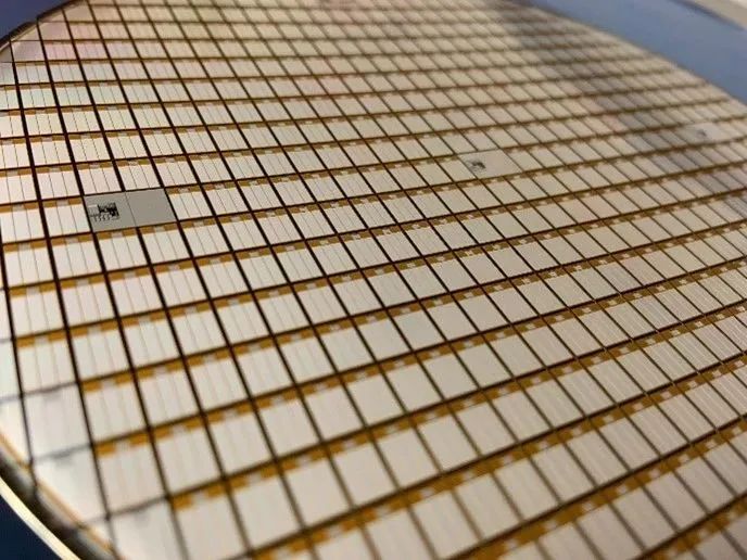
Figure 1. Wafer of SiC MOSFET with completed manufacturing and testing
The surface of the chip is generally composed of source pads, gate pads, and Kelvin source pads as shown in Figure 2. Some chips only have Gate pads, while the ones shown in the picture do not have Kelvin source pads.
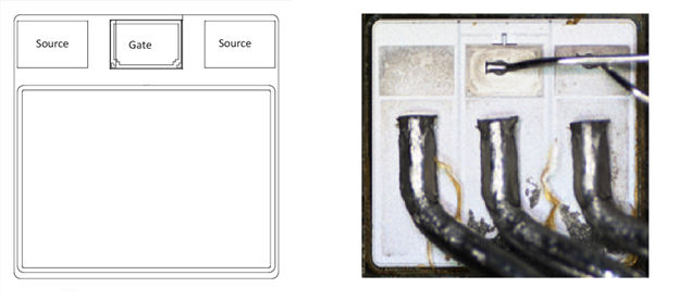
Figure 2. Chip Surface
Here we carefully observe a narrow ring around the chip, which mainly serves to enhance the chip's voltage resistance. We call it the Edge termination ring, which is usually a JTE structure. In fact, a chip is mainly composed of three parts: Terminal Ring, Gate Pad, Kelvin Source Pad, and Active Cell. The outer circle of the chip is a voltage resistant ring, and the gate pad transmits the gate signal to each cell. Inside, there are millions of active cells.
Usually, people pay more attention to Active Cells because the switching and conductivity performance of chips are mainly related to Active Cells. Here we summarize the layout of the chip and the functions and characteristics of each part, so that everyone can have a better understanding of the chip.
Pressure resistant ring
(Edge termination Ring)
The switch units surrounding the chip currently mostly adopt JTE structure;
Effectively controlling leakage current to improve the reliability and stability of SiC devices;
Reduce the electric field concentration effect and improve the breakdown voltage of SiC devices. The breakdown voltage of SiC MOSFET is related to each specific switching unit and also has a significant impact on the withstand voltage loop;
To prevent ion migration, JTE technology can be used to suppress the drift of mobile ions, thereby improving the reliability and stability of SiC MOSFETs.
In fact, the main function of the voltage withstand ring is to improve the voltage withstand of the chip. The voltage withstand of SiC MOSFET is related to Active Cell, but the field strength at the edge of the chip is very high, which can easily lead to edge breakdown. Therefore, this is the role of JTE. In some high-voltage devices, even the area of JTE may be larger than that of Active Cell.
Gate pad, Kelvin source pad
(Gate Pad, Kelvin Source Pad )
The main function of the gate pad is to transmit the gate signal to various switch units. It should be noted that the chip integrates gate resistors, which can save space and some costs in module packaging.
The Kelvin source mainly increases the switching speed and reduces switching losses. However, when used in parallel, special design is required to use it.
Switching unit
(Active Cell )
The path of current conduction and closure;
All units are connected in parallel;
Under fixed unit characteristics, the number of units determines the conduction resistance and short-circuit current capability of the entire chip;
At present, it is mainly divided into two types of structures: flat and groove.
Now, we have a better understanding of the surface layout of SiC MOSFETs. Edge terminal and Active Cell are two very important parts in SiC chips. We have rich experience in JTE design and have developed from M1 to M3 in SiC MOSFETs. Through several generations of technological iteration, JTE design simulation and manufacturing are very mature. Let's summarize some characteristics and design considerations of JTE.
SiC JTE (junction extension region) is a structure used to improve the voltage blocking capability of silicon carbide (SiC) power devices. The design of SiC JTE is crucial for achieving the required breakdown voltage and avoiding premature breakdown caused by high electric fields at the device edges.
Here are some key considerations for SiC JTE design:
1. Width and doping of JTE region: The width and doping concentration of JTE region determine the electric field distribution at the edge of the device. A wider and heavily doped JTE region can reduce the electric field and increase the breakdown voltage.
2. Cone angle and depth of JTE: The cone angle and depth of JTE affect the distribution of electric field and breakdown voltage. A smaller cone angle and a deeper JTE can reduce the electric field and increase the breakdown voltage.
3. Surface passivation: The surface passivation layer is crucial for reducing surface leakage and increasing breakdown voltage. Specially designed and optimized passivation layers are required for SiC JTE devices.
4. Thermal design: SiC JTE devices can operate at higher temperatures than their Si counterparts. However, high temperatures may also reduce device performance and reliability. Therefore, thermal design such as heat dissipation and thermal stress should be considered in the SiC JTE design process.
Overall, SiC JTE design is a complex process that involves trade-offs between various design parameters. Careful optimization and simulation are required to achieve the desired device performance and reliability.
Active Cell Switching Unit - The Core of SiC MOSFET
We can divide MOSFETs (silicon and silicon carbide) into two categories based on their gate structures: planar structures and trench structures, as shown in Figure 3. If structurally speaking, silicon and silicon carbide MOSFETs are the same, but in terms of manufacturing processes and design, due to the characteristics of silicon carbide materials and silicon materials, most of the points they need to consider are quite different. For example, SiC extensively uses dry etching and high-temperature ion implantation processes, with different implanted elements.
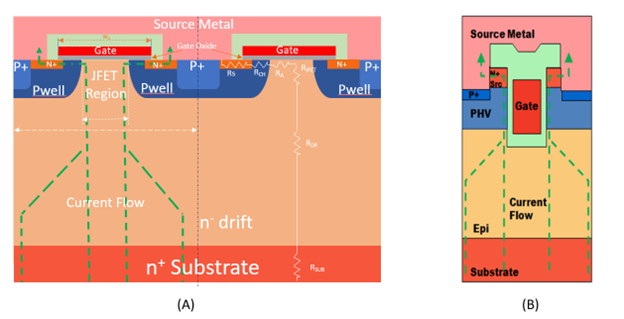
Figure 3 The planar structure and trench structure of MOSFET
The vast majority of SiC MOSFETs internationally currently use the planar structure shown in Figure 3A, with a few manufacturers adopting the trench structure shown in Figure 3B. From a development perspective, it will ultimately lead to the emergence of groove structures. However, the potential of current planar structures can still be further explored, and groove structures have not shown the level they should have. Here, we introduce a unified scale to measure their performance - Rsp (Rdson * area), which identifies the on resistance per unit area. SiC MOSFETs with planar structures have the advantages of high reliability and simple design and processing.
The Rsp of SiC MOSFETs used in automotive main drive inverters has decreased from 4.2 m Ω * cm2 in the first generation M1 to 2.6 m Ω * cm2 in M2. The current latest M3e has Rsp performance at room temperature that is consistent with the level of SiC MOSFETs with trench structures from competitors, while the Rsp at high temperatures is lower than that of SiC MOSFETs with trench structures from competitors, reaching an industry-leading level. The cell pitch value of M3e is comparable to that of SiC MOSFETs with current trench structures, indicating that the development and optimization of SiC MOSFETs with planar structures have reached a considerable level. Of course, the performance of a MOSFET not only depends on Rsp, but also on switch losses. Through the development of previous generations of SiC MOSFETs and based on extensive customer feedback, SiC MOSFET devices have been optimized for conduction loss, turn-on loss, reverse recovery loss, and short-circuit time, achieving optimal efficiency in customer applications.
The design and manufacturing direction of the planar structure Active Cell of SiC MOSFET is mainly to reduce the pitch value, increase the density of switch cells, reduce Rdson, and improve the reliability of the gate oxide layer.
In order to minimize the on resistance of the structure shown in Figure 3A, it is necessary to adjust the spacing between the switch units. The pitch value and Wg, which is the width of the gate, have a certain relationship. As the pitch value decreases, Wg also decreases accordingly, which is beneficial for the reliability of the gate. In SiC MOSFETs, the gate oxide layer is very thin, less than 100 nanometers, so dry etching is used in the SiC production process to control the processing accuracy.
According to the schematic diagram of the on resistance in Figure 3A, we can conclude that Rdson=Rs+Rch+Ra+Rjfet+Rdrif+Rsub, where Rch and Ra account for the largest proportion, exceeding 60%. Therefore, they have become one of the key directions for design and process optimization. However, simply reducing the width of the switch unit gate cannot reduce Rsp. If the width of the gate Wg is reduced to a certain range, it will actually lead to an increase in Rsp. In the design process, it is necessary to comprehensively consider the influence of the above parameters on each other in order to obtain a more reasonable optimization result. After several generations of process iteration and development, SiC MOSFETs with planar structures have developed relatively maturely in terms of performance, yield, reliability, and other aspects.
In the chip, each active cell is connected in parallel. Figure 4 is a schematic diagram of a cross-sectional view of the chip, which adopts a strip structure layout. From here, everyone will have a more vivid understanding of chips.
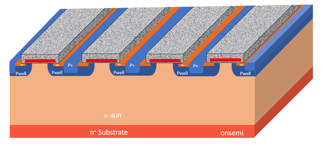
Figure 4. Cross sectional view of the chip
Here are some key considerations for the design of SiC MOSFET Rdson:
1. Channel width and doping: The channel width and doping concentration of SiC MOSFET can affect Rdson and current density. Wide and heavily doped channels can reduce Rdson and improve current carrying capacity.
2. Gate oxide layer thickness: The thickness of the gate oxide layer affects the gate capacitance, which in turn affects the switching speed and Rdson. Thinner gate oxide can improve switching speed, but it may also increase gate leakage current and increase the risk of oxide layer breakdown failure.
3. Gate design: Gate design affects gate resistance, which in turn affects switching speed and Rdson. A lower gate resistance can increase switching speed, but it may also increase gate capacitance.
Overall, the design of SiC MOSFET Rdson is a complex process that involves comprehensive consideration of the mutual influence between various parameters. Careful optimization and simulation, as well as experimentation and testing, are required to achieve the desired device performance and reliability.
Integrated on-chip gate resistor
All SiC MOSFETs developed for main drive inverters integrate gate resistors, and we can see the difference in resistance from Figure 5. Figure 5A does not require a gate resistor (integrated on the chip), while Figure 5B requires an additional gate resistor.
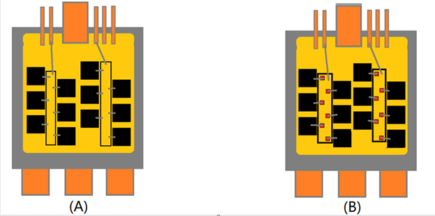
Figure 5. Difference between gate resistance and non gate resistance
Integrating gate resistors can bring some benefits to module design and manufacturing:
Simplified the process of module binding lines and reduced the failure rate.
Reduced the process of welding resistance to DBC
Reduced BOM and manufacturing costs
Relatively compact design and manufacturing for easy packaging
The design and manufacturing process of SiC MOSFET is very complex. This article briefly introduces its process and some key considerations, hoping to give everyone a concept of the design and manufacturing of SiC MOSFET.
