What is MOS transistor?
The full English name of MOSFET is MOSFET (Metal Oxide Semiconductor Field Effect Transistor), which refers to the insulated gate type of MOSFET. Therefore, MOS transistors are sometimes referred to as insulated gate field-effect transistors. In general electronic circuits, MOS transistors are commonly used in amplifier circuits or switch circuits.
1. Construction of MOS transistor
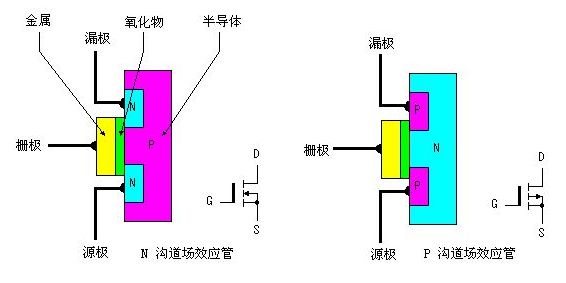
On a P-type semiconductor silicon substrate with low doping concentration, two high doping concentration N+regions are fabricated using semiconductor photolithography and diffusion processes, and two electrodes are drawn out using aluminum metal as the drain electrode D and source electrode S, respectively. Then, a thin layer of silicon dioxide (SiO2) insulation film is applied to the surface of the P-type semiconductor between the drain and source, and an aluminum electrode is mounted on this insulation film as the gate G. This constitutes an N-channel (NPN type) enhanced MOS transistor. Obviously, its gate and other electrodes are insulated from each other. A and B shown in Figure 1-1 are its structural diagram and representative symbols, respectively.
Using the same method as described above, two high doping concentration P+regions are fabricated on a low doping concentration N-type semiconductor silicon substrate using semiconductor photolithography and diffusion processes. With the same gate fabrication process as described above, a P-channel (PNP) enhanced MOS transistor is formed. The following figures show the structure diagrams and representative symbols of N-channel and P-channel MOS pipelines, respectively.

2. The working principle of MOS transistor
There are two back-to-back PN junctions between the drain D and source S of the enhanced MOS transistor. When the gate source voltage VGS=0, even with the addition of the drain source voltage VDS, there is always a PN junction in reverse bias state, and there is no conductive channel between the drain source (no current flows), so the drain current ID=0 at this time.
At this point, if a forward voltage is applied between the gate and source, i.e. VGS>0, an electric field with the gate pointing towards the P-type silicon substrate is generated in the SiO2 insulation layer between the gate and the silicon substrate. Since the oxide layer is insulating, the voltage VGS applied to the gate cannot form a current, and a capacitor is formed on both sides of the oxide layer. VGS is equivalent to charging this capacitor and forming an electric field. As VGS gradually increases, it is attracted by the positive voltage of the gate, and a large number of electrons gather on the other side of this capacitor to form an N-type conductive channel from the drain to the source. When VGS is greater than the turn-on voltage VT of the transistor (usually about 2V), the N-channel is formed. The tube begins to conduct, forming a drain current ID. We refer to the gate source voltage at which the channel begins to form as the turn-on voltage, which is generally represented by VT.
Controlling the magnitude of the gate voltage VGS changes the strength of the electric field, which can achieve the goal of controlling the magnitude of the drain current ID. This is also an important characteristic of MOSFETs that use electric fields to control current, so they are also called field-effect transistors.
3. Characteristics of MOS transistor
From the working principle of the MOS transistor mentioned above, it can be seen that the gate G and source S of the MOS transistor are insulated. Due to the presence of the SiO2 insulation layer, there is an equivalent capacitance between the gate G and source S. The voltage VGS generates an electric field, which leads to the generation of source drain current. At this point, the gate voltage VGS determines the magnitude of the drain current, and controlling the magnitude of the gate voltage VGS can control the magnitude of the drain current ID. This leads to the following conclusion:
1) MOS transistor is a device that controls current by changing voltage, so it is a voltage device.
2) The input characteristic of MOS pipeline is capacitive, so the input impedance is extremely high.


