One of the most promising devices for high-power and high-frequency applications is SiC MOSFET. It supports higher junction temperatures and features low on resistance and higher switching. SiC MOSFETs allow for the construction of converters with higher power density and higher efficiency. However, the widespread adoption of SiC MOSFETs is limited by their switching losses. Most of the losses occur during the start-up phase, as shown in the device data sheet and report test results.
The switching performance of SiC MOSFET is controlled by gate drive. Voltage source gate drive (VSG) is the most widely used structure in MOSFETs due to its low cost and simplified structure. As the gate current decreases, it can be seen that the gate voltage increases. When the Miller platform phenomenon occurs, this increase becomes constant; This situation occurs when the gate drive output voltage is at a constant rate. The entire process is shown in Figure 1. In order to improve the switching speed of power devices, it is necessary to increase the gate current 14-17 during switching transients. Therefore, a current source gate is designed. The original article can be found here.
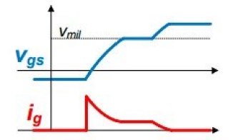
Figure 1: Gate current during transient activation
Charge Pump Gate Drive (CPG)
The limited gate current is the reason for improving the switching speed of SiC MOSFETs. In order to find a solution, further research is needed on the factors that affect the gate current between the conduction transient processes of typical VSGs. The rated gate voltage of SiC MOSFET is 20 V. The gate driver can meet two main requirements during the switching process: firstly, the gate driver should provide a sufficient amount of gate current to reduce the switching time during the switching process. Transient phase of switch. Secondly, the gate driver should be able to maintain the gate voltage in a controlled state during transient and steady-state periods.
The gate voltage should be kept below the rated value of the MOSFET. Due to the second condition, it has been noted that the gate driver power supply voltage cannot be increased. Figure 2 depicts the ideal power supply voltage for the gate driver. In order to increase the voltage, more transformers and power sources are needed, which ultimately increases the cost and complexity associated with gate driving. The 18 voltage offset requires precise control signals to avoid gate overvoltage, which not only increases the complexity of the circuit, but also cannot adaptively adapt to different load and bus voltage conditions, where the switching transient time may vary. one
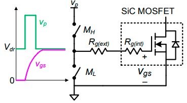
Figure 2: Gate drive with ideal voltage power supply
The working principle of CPG
There are five typical conduction switch cycles. Figure 3 shows the waveform formed during this process. When the transient conduction begins, the operation is as follows:
Subinterval 1 (t0 – t1)
Subinterval 2 (t1 – t2)
Subinterval 3 (t2 – t3)
Subinterval 4 (t3 – t4)
Subinterval 5 (t4 – t5) 1
Typical VSG and suggested CPG have similar turn off processes, as the conduction loss is much greater than the turn off loss. one
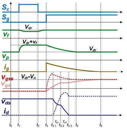
Figure 3: CPG waveform
Control signal generation
The suggested CPG requires two control signals, which can be easily confirmed through a combination of PWM input signals and several logic gates. Figure 4 shows the confirmation of the basic principle of the proposed CPG for control. Delay units can be executed using RC filters with various values. one
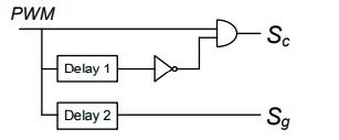
Figure 4: Implementation of CPG Control Logic
The benefits and challenges of the proposed CPG
The advantages include low switching losses during the turn-on phase, as the gate current charging the gate capacitor during the turn-on transient is higher. Compared to traditional VSG, this is achieved by driving the output voltage through the pump gate. The charging voltage that has been pumped has decreased back to the normal gate power supply voltage. This will ultimately avoid any type of overcharging. The turn-on switch speed of SiC MOSFET can be easily adjusted by changing the external gate resistance. Therefore, it is convenient to replace the traditional VSG in the power converter with the recommended CPG. Its challenges include charge storage capacitor voltage and higher dV/dt.
Parameter design
It is important to choose the appropriate capacitor C P when designing the proposed CPG. Figure 5 shows the waveforms of siphon voltage V P and external gate to ground voltage (V gse+V n) with different C P values. During the transient conduction period, C P transfers charges to C GS.
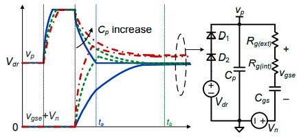
Figure 5: Voltage waveforms during the turn-on phase of different Cps
experimental result
With the help of Wolfspeed's most advanced chip technology, SiC MOSFET was used to test the proposed CPG, as shown in Figure 6. Tables 1 and 2 show the parameters related to CPG and the characteristics of MOSFETs.
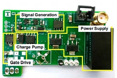
Figure 6: Prototype of CPG

Table 1: Characteristics of Silicon Carbide MOSFET
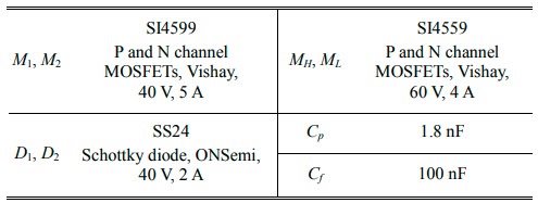
Table 2: Gate Drive Parameters
conclusion
This article introduces a CPG driver that can improve the on/off losses of SiC MOSFETs. A comparison has been made between the proposed CPG and traditional VSG. The results of this experiment indicate that the conduction loss value of the proposed CPG has been reduced by 71.7%, while the switching time under full load conditions has been reduced by 67.4%.


